Reports: DNI1053270-DNI10: Rapid-Thermal Catalytic Conversion of Petroleum Products into Multilayer Graphene
 printer friendly
The objective of the project is to explore a novel synthesis approach based on the rapid-thermal catalytic conversion of petroleum products into multilayer graphene. This new approach establishes a fundamental understanding of how defects are formed during the graphene conversion process as well as defect mitigation strategies. With the support from ACS Petroleum Research Fund, we successfully accomplished three main tasks throughout this project: (i) the development of metal alloy catalysts for homogeneous catalytic conversion of low quality carbon products into multilayer graphene, (ii) rapid-thermal conversion to minimize defects during graphene synthesis, and (iii) controlling the amount of the solid-state source to improve the consistency and efficiency of conversion, each of which are described in further detail throughout this report. These developments have been published in leading journals in the field and have solidified Principal Investigator’s (PI) research expertise in the area of graphene synthesis and manufacturing. The support from ACS Petroleum Research Fund has also provided direct support to two graduate students in PI’s lab.
1. Development of Metal Alloy Catalysts
We achieved the systematic and precise synthesis of multilayer graphene ranging from 3.5 to 35 nm by selectively patterned cobalt (Co) with varying thicknesses on a copper (Cu) film via low pressure chemical vapor deposition (LPCVD).
Figure 1 shows optical microscope images of graphite (letters) and graphene (background) synthesized on different catalyst metals. Vowel letters (i.e. Es) in Figure 1a are composed of thicker graphite (~23 nm) synthesized on a thicker Co (750 nm) while consonants (i.e. M, C, H, and S) are composed of thinner graphite (~4 nm) synthesized on a thinner Co (200 nm). Letters in Figure 1b are composed of ~30 nm thick graphite synthesized on a 900 nm thick Co. For both Figure 1a and 1b, the background is bi- or tri- layer graphene which was synthesized on a 700 nm Cu thinfilm.
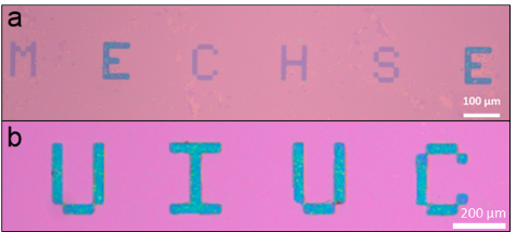
Figure 1. Synthetic control of multilayer graphene. (a) Consonants are composed of thinner graphite (~4 nm) and the vowel is composed of thicker graphite (~23 nm). (b) All letters are composed of ~30 nm thick graphite.
Figure 2 shows Raman characterizations to demonstrate thickness and quality control. Graphene and graphite has three distinctive bands in Raman spectrum: D band (at ~1,350cm-1), G band (at ~1,590cm-1) and 2D band (at ~2,690cm-1). The thicker graphite is confirmed by a small Raman I2D/IG ratio (<0.5) whereas bi-/tri-layer graphene shows a I2D/IG ratio close to 2. Figure 2b demonstrates the homogeneity of graphite cross pattern by Raman 2D mapping of I2D/IG ratio.
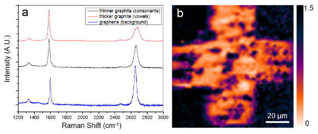
Figure 2. Raman spectroscopic analysis. (a) Raman spectra of graphite and graphene with different thicknesses from Figure 1a. (b) Raman I2D/IG mapping of synthesized graphite.
2. Development of Rapid-thermal Conversion
We developed a rapid-thermal conversion for graphene growth. A microcombustion system shown in Figure 3a and 3b was developed for the conversion process with rapid heating and cooling rates as well as minimal catalyst dewetting which often occurs in a conventional CVD process.
Oxygen is used as an oxidizer and hydrogen is used as a fuel. A flame is stabilized at the center of the gas channel (Figure 3b) and provides heat to a Cu foil during the synthesis. The desired graphene synthesis site is marked as a shaded oval which is on the opposite side of the flame as shown in Figure 3c.
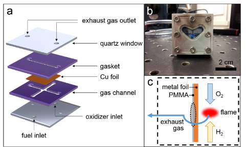
Figure 3. (a and b) Schematic diagram and photo of the developed rapid thermal conversion setup. (c) Flame occurs at the mix zone of oxidizer and fuel. The shaded oval is the desired site for graphene/graphite synthesis.
With this rapid-thermal setup, graphene synthesis was carried out using a thin poly(methyl methacrylate) (PMMA) as a solid-state source. Raman characterization (Figure 4) shows the quality of graphene synthesized by this method. 0.1% PMMA solution in anisole was spin coated on a 25 µm thick Cu foil and the graphene was synthesized on the Cu surface. The Raman spectrum in Figure 4a shows I2D/IG ≈ 2, suggesting the presence of graphene with a small D band which indicates existence of minimal defects in the synthesized graphene. To synthesize multilayer graphene, 10% PMMA solution was spin coated on a 50 µm thick Ni foil. The Raman spectrum in Figure 4b demonstrates the few layer graphene with small defect levels.

Figure 4. Raman spectra of graphene and multilayer graphene synthesized by the rapid-thermal conversion setup. (a) Single layer graphene synthesized on a 25 µm Cu foil. (b) Multilayer graphene synthesized on a 50 µm Ni foil.
3. Control of the Amount of the Solid-state Sources
We demonstrate a controlled multilayer graphene synthesis strategy by modulating the amount of the solid-state carbon source. Figure 5 shows the process of rapid thermal CVD synthesis of graphene on a SiO2/Si substrate.
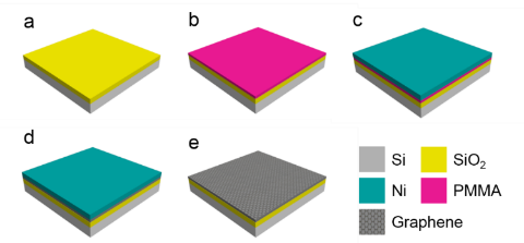
Figure 5. Rapid thermal synthesis process of graphene from a solid-state carbon source: (a) preparation of a clean SiO2/Si substrate, (b) spin coat PMMA, (c) Ni deposition, (d) high-temperature annealing for graphene growth, and (e) Ni wet etch.
We studied the effect of various synthesis parameters to optimize the graphene thickness and quality. Figure 6a shows Raman spectra of graphene films acquired from two different solid-state carbon sources. The quality of the graphene film strongly depends on the annealing temperature as shown in Figure 6b. The highest quality of graphene film was synthesized at 1000 ºC, characterized by Raman D band intensity. We varied the PMMA concentration in anisole between 0.1-0.4 wt% to control the amount of the solid carbon source (Figure 7a). The number of graphene layers increased with the amount of solid carbon source, characterized by Raman I2D/IG ratio (Figure 7b).
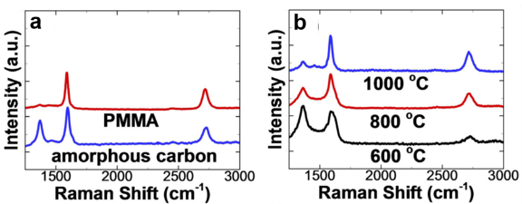
Figure 6. Raman spectroscopic analysis of graphene to find a proper carbon source and optimum temperature condition. (a) Raman spectra of multilayer graphene grown from different solid-state carbon sources. (b) Raman spectra of multilayer graphene acquired from various annealing temperatures.
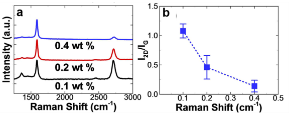
Figure 7. Raman spectroscopic analysis to show graphene thickness controllability. (a) Raman spectra of multilayer graphene acquired from various PMMA concentrations. (b) I2D/IG of multilayer graphene synthesized from varying PMMA concentrations.