Reports: ND1053741-ND10: Stress Corrosion Cracking in Ultrafine Grained Ni and Its Alloy for Petrochemical Industries
 printer friendly
Annual project report (Jan. 1, 2014-Aug. 31, 2015)
1. Objective
The objectives of this proposal are two folds: (1) evaluate corrosion/stress corrosion cracking (SCC) resistance of a coarse grained (CG) and ultrafine grained (UFG) Ni and C22HS Ni alloy (Hastealloy) in sour environment (CO2 and H2S) for applications in petrochemical industry, and (2) elucidate the mechanism of H2 embrittlement and stress corrosion cracking in CG vs UFG Ni and C22HS Ni alloys.
2. Brief summary of major findings
In this fiscal year, pulse electrodeposition (PED) has been successfully employed to fabricate various nanocrystalline (nc) Ni coatings on 304 stainless steel (304SS) plates to imitate practical utilization of coatings for petrochemical application. The Ni coatings are well bonded to substrates. The grain size of nc Ni coatings proved to be controllable over a wide range, from 1.0 µm to 48 nm, by tailoring mean current density. The nanoindentation results suggest a strong dependence of hardness on the average grain size. The nc Ni yields the hardness of ~ 6 GPa at an average grain size of 48 nm due primarily to grain boundary strengthening.
3. Detailed description of major findings
Ni coatings were electrodeposited on 304 stainless steel substrates at 45 ℃ using a galvanostat (Dynatronix) with a DPR 40-30-100 pulsed power supply, and a nickel plate was used as anode. The pulse-on/off duration was controlled as 2 ms/2 ms. The current density varied from 2 to 10 A/dm2 to adjust the grain size. An FEI Tecnai G2 F20 ST transmission electron microscope operated at 200 KV was employed to examine the microstructure of coatings. Scanning electron microscopy studies were performed on a JEOL JSM-7500F field emission scanning electron microscope (with 5 nm resolution). Hardnesses and elastic modulus of the specimens were measured using a Fischerscope 2000XYp nano/microindenter. The x-ray diffraction (XRD) patterns of as-deposited coatings were recorded using a PANalytical Empyrean XRD diffractomer.
A very good adhesion between the functional coatings and substrates is essential. SEM image of mechanically polished 304 SS substrate in FIG. 1a shows significant surface roughness. After electropolishing, the rough surface profile was effectively removed (FIG. 1b).
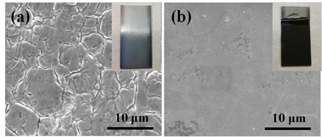
FIG. 1. SEM images of the 304 stainless steel substrates (plates) (a) prior to and (b) after anodic electrodepolishing. The inset is the corresponding optical image of the coated plates.
Nc Ni coatings were electrodeposited by varying peak current density and pulse-on/pulse-off procedures. The mean current densities of 2-10 A/dm2 were applied. FIG. 2 clearly shows the surface morphology of two typical as-deposited Ni coatings prepared at 2 and 10 A/dm2, respectively. Grain boundaries can be recognized for the Ni coatings deposited at 2 A/dm2. In contrast, the Ni at 10 A/dm2 exhibits a less rough surface. The PED in our case yielded a high deposition rate of ~1.1 μm/min, indicating its potential for industrial applications.
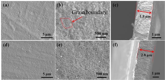
FIG. 2. (a) low magnification plan-view, (b) high magnification plan-view, and (c) cross-sectional SEM images of the Ni coating prepared at a current density of 2 A/dm2. The circulated dash line in Fig. 2b indicates the grain boundary. (d) Low magnification plan-view, (e) high magnification plan-view and (f) cross sectional SEM images of the Ni coating prepared at a current density of 10 A/dm2.
The typical plan-view TEM images for some typical electrodeposited nc Ni coatings are shown in FIG. 3. The average grain size for Ni coating prepared at 2, 6, 8, 10 A/dm2 is 1 μm, 720 nm, 362 nm and 48 nm, respectively. A greater current density leads to smaller average grain size. Furthermore this technique enables us to tailor the average grain size over an order of magnitude.
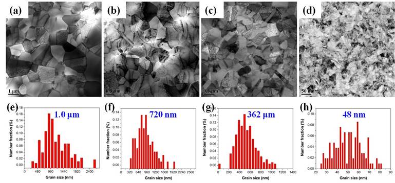
FIG. 3. Plan-view bright field TEM micrographs illustrating the grain size evolution of Ni coatings fabricated at a current density of (a) 2 A/dm2, (b) 6 A/dm2, (c) 8 A/dm2 and (d) 10 A/dm2. Grain size distribution charts show the average grain sizes of Ni coatings fabricated at a current density of (a) 2 A/dm2, (b) 6 A/dm2, (c) 8 A/dm2 and (d) 10 A/dm2 vary drastically from 1 µm to 48 nm.
The XRD patterns in FIG. 4 reveal that the PED Ni coatings are polycrystalline and possess face-centered cubic (fcc) structure with dominant (111) and (200) diffractions. The INi(111)/INi(200) ratio gradually increases at a higher current density.
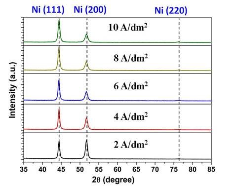
FIG. 4. XRD patterns of the Ni coatings prepared at various current density. The films have prominent (111) and (200) peaks.
FIG. 5 shows the nanoindentation hardness of the different Ni coatings as a function of indentation depth. The hardness for all the specimens reaches a plateau at the range of 150-350 nm. In the plateau region, the mean hardness for all the Ni coatings was calculated and plotted as a function of grain size. The maximal hardness is ~ 6 GPa for the nc Ni with 48 nm grain size. The high hardness is an indication of good wear resistance in nc Ni coatings.
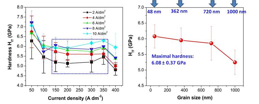
FIG. 5. A plot of indentation hardness versus indentation depth for the Ni coatings prepared at various current densities. The mean hardness is plotted as a function of grain size.
Future activities
1. Perform systematic corrosion and wear tests on the nc Ni coatings.
2. Apply ECAP to process C22HS Ni alloys and refine the grain size of these alloys
3. Investigate corrosion resistance of C22HS Ni alloys
4. Explore stress corrosion cracking resistance of C22HS Ni alloys
Impact on the personnel
This project allows the PI to develop strong collaboration with Schlumberger. Furthermore the PI’s grad and undergrad students are directly involved in industrial projects and are trained to perform high quality research. The results derived from these studies will be published as journal articles. Also the PI and his grad students will present the research at national conferences.