Reports: DNI555709-DNI5: Surface Chemistry of Few Layer Hydrodesulfurization and Hydrodenitrogenation Catalysts on Sapphire Imaged by Atomic Force Microscopy
 printer friendly
Oil and gas supplies comprise many chemicals which must be separated prior to using the hydrocarbons as chemical feedstocks. In particular, sulfur containing molecules such as thiophenes, an nitrogen containing molecules such as amines and N-heterocycles must be removed prior to cracking long chain alkanes because they can poison the cracking catalysts. The conventional method for removing sulfur and nitrogen in petroleum feedstocks is hydrotreating reactions such as hydrodesulfurization (HDS) and hydrodenitrogenation (HDN).
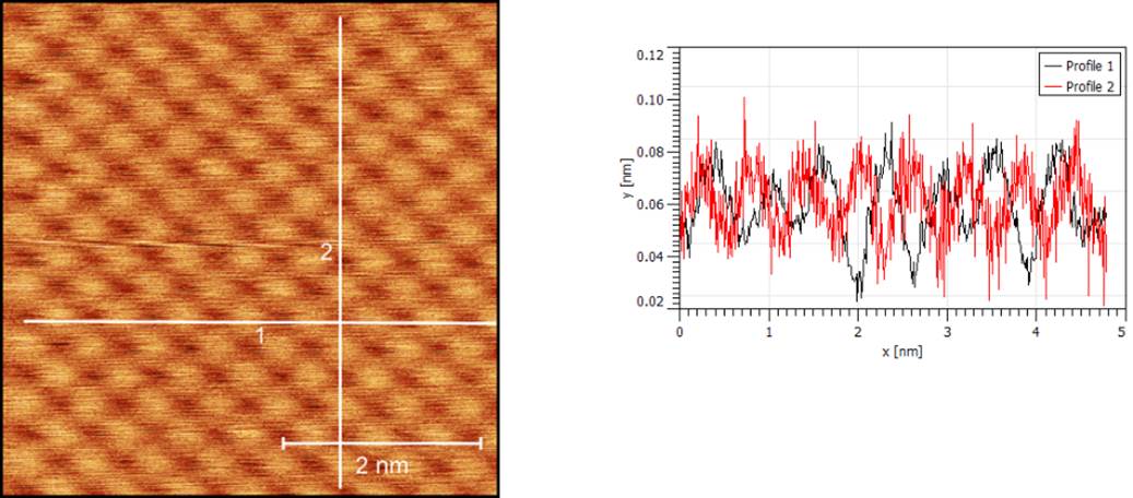
Figure 1 Atomically Resolved AFM image of NaCl aquired in our lab at 10 K. Right: Light profile illustrating noise levels at 0.08 nm rms.
The goal of our research proposal is to study the structure and reaction pathways of MoS2 and WS2 catalysts used in this reaction. These materials are commonly used in nanoparticle form on a ![]() -alumina support. These are layered materials, and recent research has shown that that the electronic structure, and therefor chemical reactivity, of these materials is highly layer dependent. New developments in chemical vapor deposition has enabled the synthesis of these catalytic materials while controlling the number of layers and enabling the formation of chemical bonds between MoS2 and WS2, mimicking the formation of co-catalysts.
-alumina support. These are layered materials, and recent research has shown that that the electronic structure, and therefor chemical reactivity, of these materials is highly layer dependent. New developments in chemical vapor deposition has enabled the synthesis of these catalytic materials while controlling the number of layers and enabling the formation of chemical bonds between MoS2 and WS2, mimicking the formation of co-catalysts.
During the first year of this grant, our research has been focused on synthesizing the materials for these interfaces, and increasing the sensitivity of UHV, q-plus atomic force microscope to achieve atomic resolution on these materials. These layered materials have neither dangling bonds at the surface and are not highly charged, so the forces pulling on the AFM tip are quite weak. The first step in this project was to demonstrate atomic resolution in UHV on a sample with large forces, NaCl, shown in figure 1. As shown in figure 1b, the lowest noise we achieved for most of the grant period in AFM is ~0.08 nm r.m.s. at 10 K. We have been working with the company (ScientaOmicron) and have installed a new microscope this summer, and our current noise is level is 0.002 nm, which should be sufficient to image individual atoms in CVD MoS2.
While we have been increasing our capabilities in scanning probe, our synthesis of MoS2 based catalysts has made great progress. Research Aim III of our proposal is to image molecules bound to nanoplates of MoO2-MoS2. In the past twelve months, we have made significant progress in understanding how to controllably grow these interfaces. We now understand that the growth of these nanoplates is governed by the chalcogenide flux during CVD growth as shown in Figure 1. When the sulfur flux is reduced, MoO2 platelets are nucleated on the surface, and the top layers are subsequently sulfurized to form the MoS2 layers. This structure is interesting because the oxide core is metallic, providing a reservoir of electrons to be used in catalytic chemistry. Furthermore, by understanding the nucleation mechanism for these nanoparticles, we have been able to control how they interface with the underlying substrate.
A small distortion of the lattice constant of the oxide core leads to a hexagonal structure which is compatible with epitaxial growth of MoO2 on Al2O3(0001), and with a ![]() R30 reconstruction of SiC(0001) (confirmed by Low Energy Electron Diffraction). We know that the growth of the nanoparticles is being controlled by the interfacial chemistry because the resulting structures are aligned along high symmetry crystallographic planes of the substrate. In both cases, we see two families of plates in scanning electron microscopy, plates that are normal to the surface, and plates that are tilted by ~35o. Each family of platelets possesses 60o rotational symmetry, and the two families are aligned at 30o relative to each other, as shown in figure 4. Furthermore the classification of two families of platelets was confirmed by locked-couple X-ray diffraction which showed only two peaks for the {010} and {001} family of MoO2 planes (figure 5). Based on the XRD data, the crystal structures, of MoO2, sapphire, and
R30 reconstruction of SiC(0001) (confirmed by Low Energy Electron Diffraction). We know that the growth of the nanoparticles is being controlled by the interfacial chemistry because the resulting structures are aligned along high symmetry crystallographic planes of the substrate. In both cases, we see two families of plates in scanning electron microscopy, plates that are normal to the surface, and plates that are tilted by ~35o. Each family of platelets possesses 60o rotational symmetry, and the two families are aligned at 30o relative to each other, as shown in figure 4. Furthermore the classification of two families of platelets was confirmed by locked-couple X-ray diffraction which showed only two peaks for the {010} and {001} family of MoO2 planes (figure 5). Based on the XRD data, the crystal structures, of MoO2, sapphire, and ![]() SiC(0001), we proposed the structure shown in figure 6 as the interfacial structure between the MoO2 cores and the substrate. This interface is particularly interesting for the SiC structure. We have reproduced these core-shell particles on highly doped SiC, and have arranged with Aaron Massari’s lab to borrow a potentiostat to perform electrochemical dehydrogenation of thiophene.
SiC(0001), we proposed the structure shown in figure 6 as the interfacial structure between the MoO2 cores and the substrate. This interface is particularly interesting for the SiC structure. We have reproduced these core-shell particles on highly doped SiC, and have arranged with Aaron Massari’s lab to borrow a potentiostat to perform electrochemical dehydrogenation of thiophene.
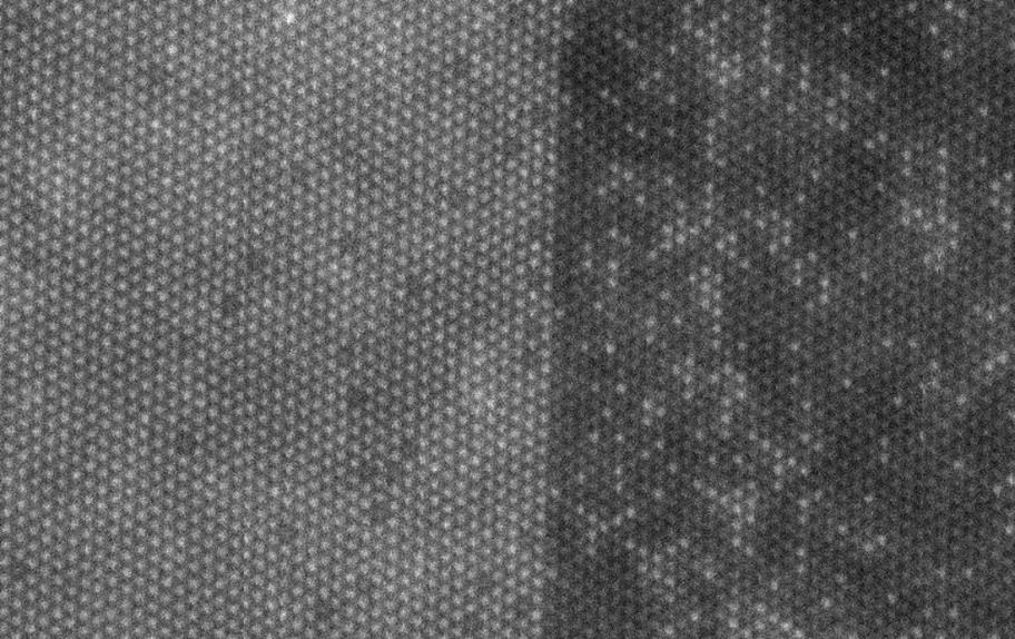
Finally, while we continue to improve our imaging performance on our q-plus AFM, we have also turned to transmission electron microscopy to image these materials. Here, we are focused on goal of imaging activating metals embedded in the MoS2 matrix. We started by synthesizing in-plane heterostructures of MoS2 and WS2 that are still monolayer thickness. We then characterized the interface using an aberration corrected TEM in HAADF mode. This allowed us to distinguish between W and Mo based on atomic number contrast, and allowed us to image individual W atoms which had diffused into the MoS2 layer (Figure 7). We will be able to use this same method to image Co and Fe atoms embedded in MoS2, to atoms commonly used to activate hydrodesulfurization. We hope to further shed light on how they increase the reaction rate by performing electron energy loss spectroscopy and measuring the electronic structure of the embedded defect.
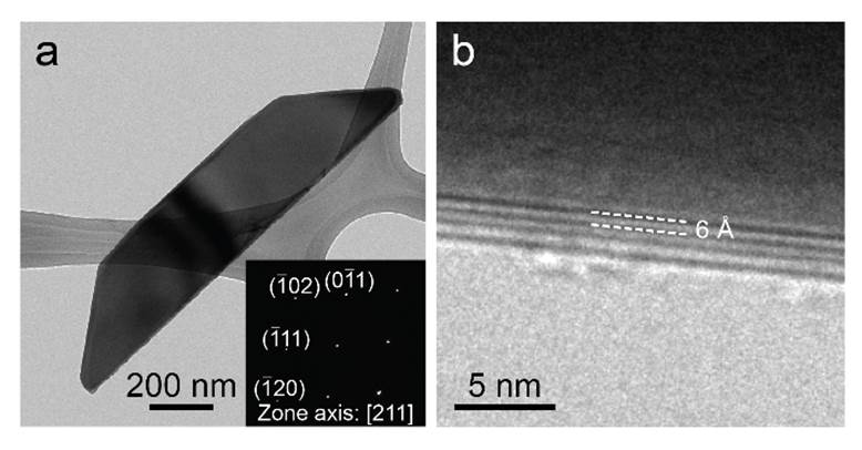
Figure 2 Schematics illustrating the self-seeding mechanisms of (a) mono-layer TMDCs (previously reported) and (b) core/shell nanoplates (reported here). (c) Raman spectra of MoO2/MoS2 core/shell plates on SiC, MoO2/MoS2 core/shell plates on sapphire, and MoO2/MoTe2 core/shell plates on sapphire with identities indicated with a symbol above each peak
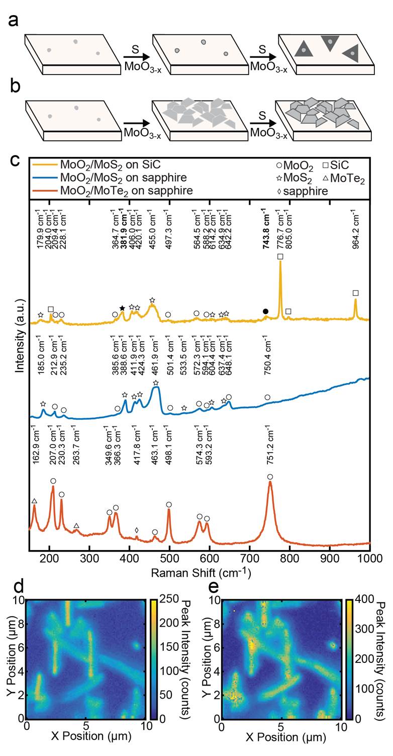
Figure 3 Transmission Electron Microscopy of MoO2/MoS2 core/shell nanoplates. The cross-sectional fringes indicate 4 layers of MoS2
![]()
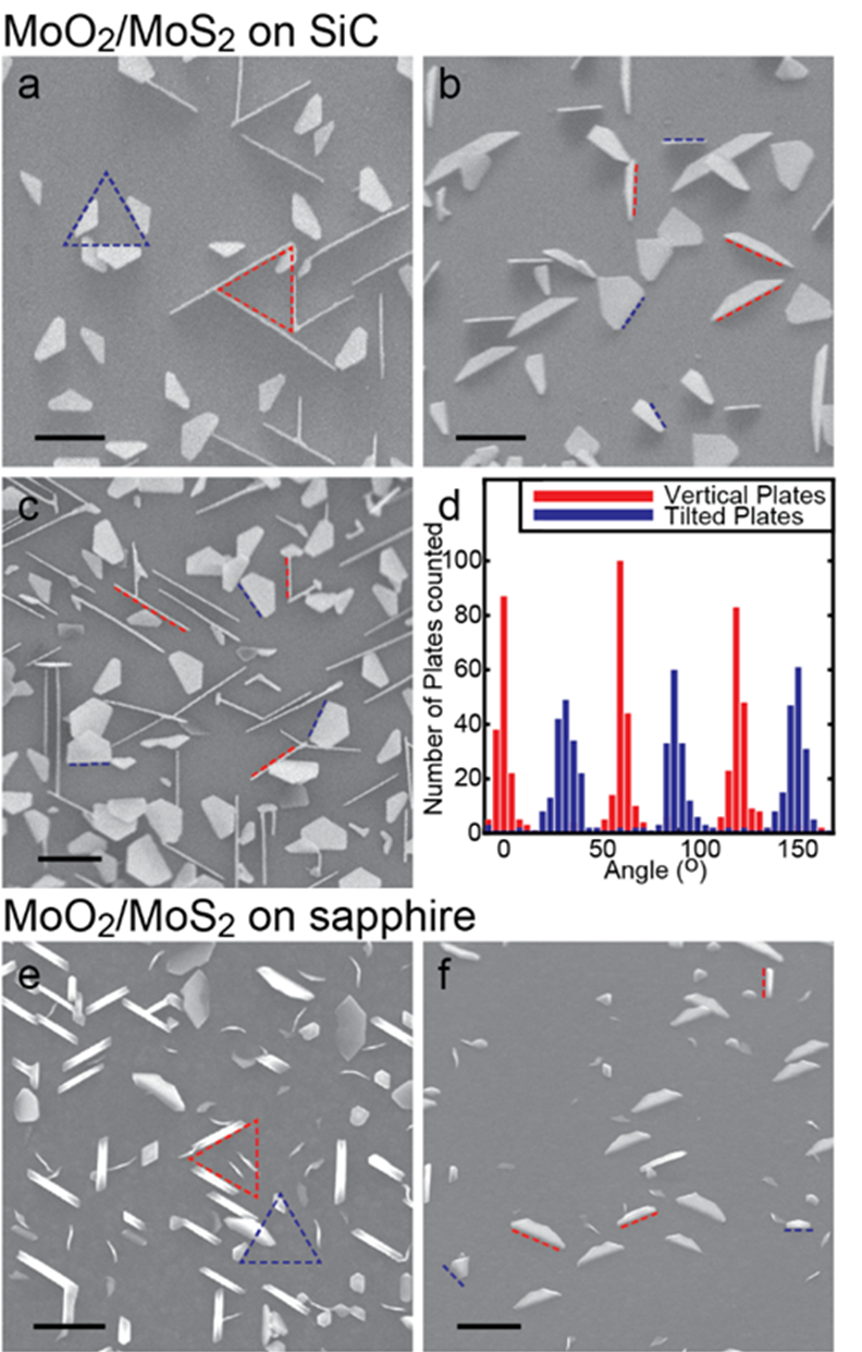
Figure 4: SEM images of MoO2 MoS2 on SiC and Sapphire substrates. Figure d: Histogram of rotational alignment of the two platelet families
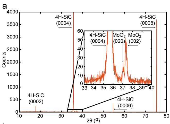
Figure 5 Lock coupled XRD scan of core/shell MoO2/MoS2on SiC(0001) showing 2 diffraction peaks.
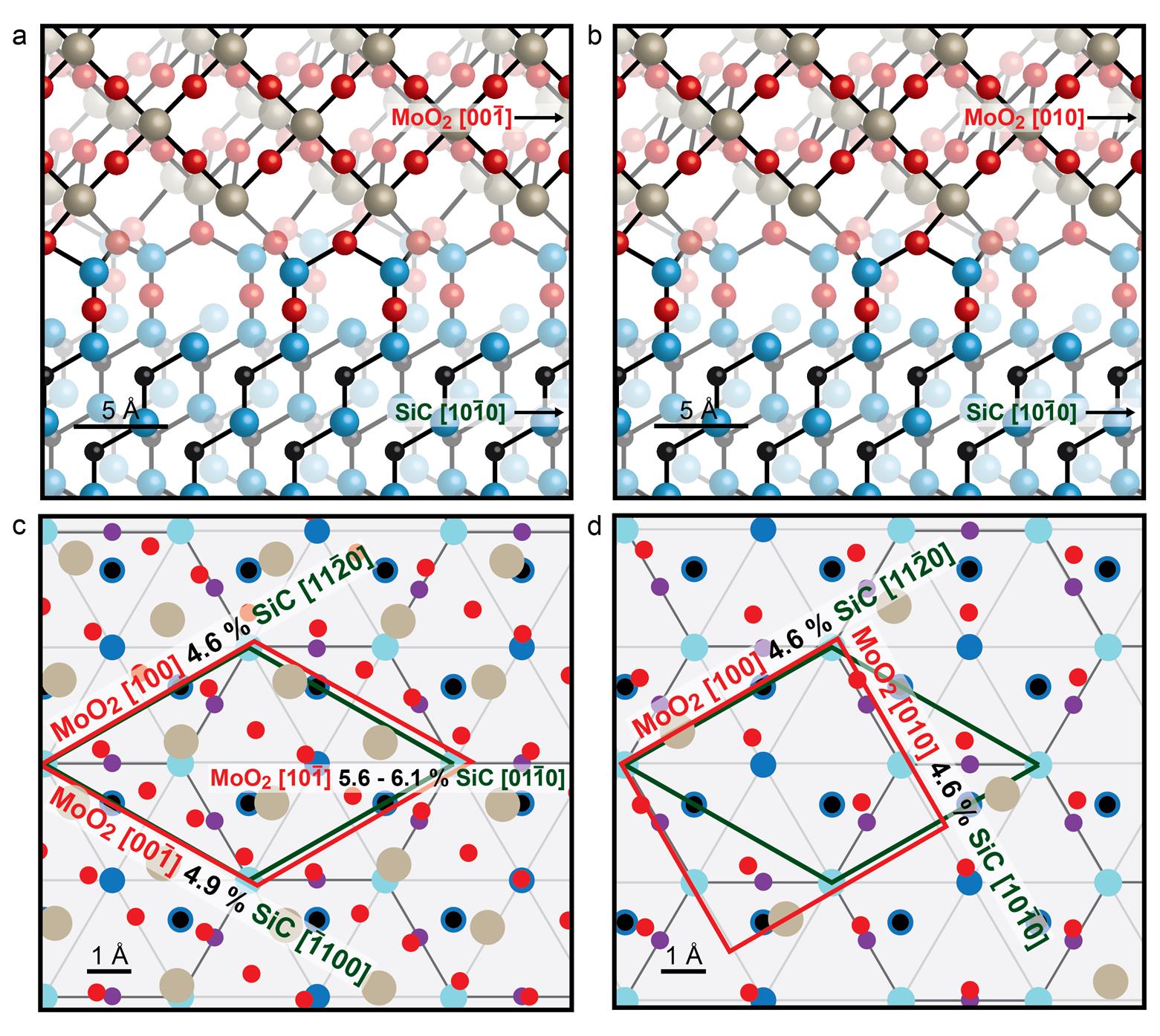
Figure 6. Proposed epitaxial relationship between MoO2(010) andMoO2(001) and SiC(0001)
Figure 7 High Angle Annular Dark Field Transmission Electron Microscope image of MoS2/ WS2 interface. Light circles are W, dark circles are Mo