Reports: ND555524-ND5: Atomically Thin Size Exclusion Membranes
 printer friendly
SCOPE AND PURPOSE
Zeolite-based membranes have been studied as size and shape-selective membranes for separations; however, low permeance has limited their application.1 The discovery of 4.3 Å thick 2D SiO2 bilayers with molecule-sized pores unlocks the potential for many orders of magnitude higher permeances while preserving the separation factor; the atomically thin nature and porosity in excess of 50% suggest such membranes approach the physical limit. While these films have only been grown on atomically flat metal substrates,2,3 the 2D bilayer is a van der Waals material similar to graphene and thus may be delaminated to produce a freestanding film with no dangling bonds. By tuning the ring structure of the SiO2 bilayers, separation of small molecule mixtures may be realized. The overall goals of this project are to synthesize bilayer silica with controlled ring size distributions, achieve transfer of the films to a suitable grid substrate, and measure the size and shape-selective transport of target gas mixtures at the limit of membrane thickness.
RESEARCH PROGRESS
Substrate Design
Crystalline SiO2 bilayers arrange in a hexagonal array of six-membered rings consisting of corner-sharing SiO4 tetrahedra, with an unstrained lattice constant close to 5.3 Å.4 While crystalline SiO2 bilayers have been successfully grown on Ru(0001) and Pd(100),2,3 significant strain-induced defects and motifs including larger rings (as large as nine-membered) are present due to the lattice mismatch. A promising way to produce “zero-strain” SiO2 bilayers with only six-membered rings is through growing the SiO2 layer on Ni-Pd alloy thin films, which are continuously tunable over a range of induced strain from 6.0% compressive to 3.8% tensile. We have developed a method for growing atomically flat (111) surfaces of the Ni-Pd alloys over a range of lattice constants by epitaxial growth on Cr2O3(0001)/α-Al2O3(0001) substrates, as represented by the characterization results in Figure 1. Compared to single crystal materials, these metal thin films are very inexpensive and may be treated as consumables for our goal of freestanding SiO2.
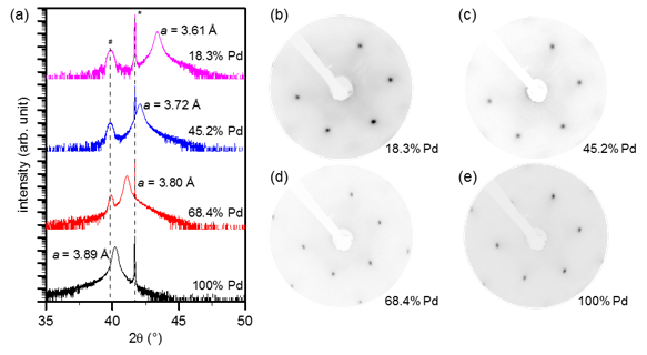
Figure 1: Characterization of Ni-Pd (111) alloy substrates grown on Cr2O3(0001)/α-Al2O3(0001). (a) XRD of the substrates with varying Pd percent, and corresponding LEED patterns ((b)-(e)) recorded at 130 eV electron energy. (*: α-Al2O3 (0006) reflection, #: Cr2O3 (0006) reflection)
SiO2 Growth on Alloy Substrates
Using the developed Ni-Pd alloy system, we then synthesized a SiO2 bilayer film on a substrate designed to induce close to zero strain. The characterization results are shown in Figure 2. LEED indicates a sharp (2x2) pattern indicating a crystalline film, with no sign of an amorphous ring as has always been seen previously on pure metal substrates where there is substantial tensile strain.5 The Ni-Pd alloy lattice constant was 3.72 Å, and so the SiO2 bilayer was subjected to 0.74% compressive strain relative to freestanding SiO2. Concurrent work on depositing SiO2 on substrates with tensile strain as low as 0.90% has been shown to induce partially amorphous SiO2, consisting of larger rings to accommodate the strain. This is the first demonstration of the effects of compressive strain on the SiO2 bilayer growth, and of inducing crystallinity high enough to enable selective gas permeation.
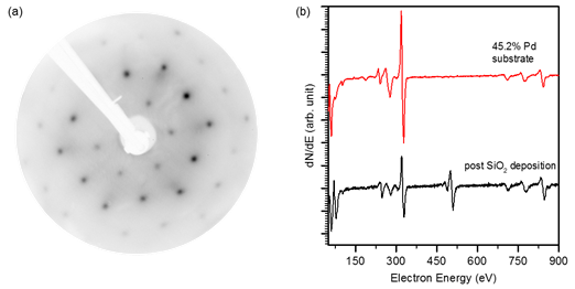
Figure 2: (a) LEED pattern (130 eV) of a crystalline SiO2 bilayer grown on a Ni-Pd (111) alloy substrate with 45.2% Pd, and (b) Auger spectra recorded before and after SiO2 deposition showing the appearance of Si (76 eV) and O (503 eV).
Bilayer Lift-off and Membrane Permeation Test System
After successfully growing the highly crystalline SiO2 bilayer required for ensuring only molecules with kinetic diameters below 2.8 Å may permeate, we began experiments to determine appropriate delamination conditions for obtaining a freestanding bilayer. As the film is invisible to the naked eye, we first spin PMMA to aid in transfer. As the Ni-Pd films are inexpensive, our first experiments involved etching the metal, leaving the SiO2 attached to only the PMMA. Since this method is inconsistent, we switched to a more promising electrochemical method. At present, we are investigating this method combined with lithography to obtain multiple test samples per film and enable stacking to cover possible breaks.
In preparation for the freestanding film, we have constructed the membrane permeation test system in Figure 3. The device allows the flow of a desired analyte gas mixture and SF6 carrier gas (5.5 Å kinetic diameter) to either side of the freestanding membrane suspended on holey transmission electron microscopy grids, with the ability to measure both permeate and retentate composition with on-line mass spectrometry. Work is ongoing to realize the size and shape-selective separation of gases with tuned bilayer SiO2 ring distributions.
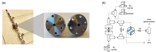
Figure 3: (a) Photograph of the membrane test system; the test grid is sandwiched between the flanges on the right. (b) A schematic of the test system operation.
SIGNIFICANCE
In the first year of this project, we have laid the groundwork for creating atomically thin membranes of bilayer SiO2 for shape and size-selective separation of gases. The development of a highly crystalline bilayer consisting of six-membered rings with no amorphous character through tuning the strain induced by the substrate is a critical milestone, as this is required for demonstrating the ability to pass only He, NH3, or H2O through the membrane. Expanding to films with eight-membered rings through further tuning will allow for more detailed study of industrially-relevant gas separation.
REFERENCES
(1) Kulprathipanja, S. Zeolites in Industrial Separation and Catalysis; John Wiley & Sons, 2010.
(2) Löffler, D.; Uhlrich, J. J.; Baron, M.; Yang, B.; Yu, X.; Lichtenstein, L.; Heinke, L.; Büchner, C.; Heyde, M.; Shaikhutdinov, S.; Freund, H.-J.; Włodarczyk, R.; Sierka, M.; Sauer, J. Phys. Rev. Lett. 2010, 105 (14), 146104.
(3) Altman, E. I.; Götzen, J.; Samudrala, N.; Schwarz, U. D. J. Phys. Chem. C 2013, 117 (49), 26144–26155.
(4) Huang, P. Y.; Kurasch, S.; Srivastava, A.; Skakalova, V.; Kotakoski, J.; Krasheninnikov, A. V.; Hovden, R.; Mao, Q.; Meyer, J. C.; Smet, J.; Muller, D. A.; Kaiser, U. Nano Lett. 2012, 12 (2), 1081–1086.
(5) Shaikhutdinov, S.; Freund, H.-J. Adv. Mater. 2013, 25 (1), 49–67.