Reports: ND1051458-ND10: New Insights on High Performance Anodes for Lithium-Ion Batteries
 printer friendly
In Year 2, we continued our project by researching the lithiation of SnO2 nanowires. Taking advantage of an aberration-corrected scanning transmission electron microscopy (STEM), we show that the dynamic lithiation process of anode materials can be revealed in an unprecedented resolution. Atomically resolved imaging of the lithiation process in SnO2 nanowires illustrated that the movement, reaction and generation of  mixed dislocations leading the lithiated strips effectively facilitated lithium ion insertion into the crystalline interior. The geometric phase analysis and density functional theory simulations indicated that lithium ions initial preferring to diffuse along [001] direction in the {200} planes of SnO2 nanowires introduced the lattice expansion and such dislocations behaviors. At the later stages of lithiation, the Li-induced amorphization of rutile SnO2 and the formation of crystalline Sn and LixSn particles in Li2O matrix were observed.
Figure 1 shows the structure and chemistry of the reaction front in a partially lithiated SnO2 nanowire. The lithiated and unlithiated sections of the nanowire are separated by dark dotted line in Figure 1a. Interestingly, we observed many dark-contrast strips emitting towards the unlithiated part of the nanowire as the lithiation reaction front moved forward. It seemed the crystalline-to-amorphous phase transformation of the nanowire started with a long-range diffusion of lithium ion across the crystalline SnO2. Figure 1b shows the SAED pattern taken with the  zone axis from the section of nanowire marked as B. In the SAED pattern, weak arcs around the {211} diffraction spots can be seen and the {020} diffraction spots are split, which indicates the lithiation-induced poly-crystallization and lattice defects. Different contrasts between the dark strips and the SnO2 crystalline part are clearly visible by high-angle annular dark field (HAADF) imaging of area B as shown in Figure 1c. Since the image intensity in a HAADF image is proportional to the atomic number (Z) (more specifically to Z1.7), the bright strips in Figure 1c should be dominated by the Sn atomic columns, while the areas with lower image intensity can be correlated to the intercalation of lithium ion and the associated disorder of the tin atomic columns. The lattice inside the strips became indiscernible and some strips (marked in the corner of Figure 1c) seemed to merge with one another. The corresponding bright field image (Figure 1d) provides more direct evidence that the lattice in the dark strips is almost amorphous. Analysis of electron energy loss spectroscopy (EELS) data (Figure 1f-g) taken from the lithiation strips indicates that the dark strips and the adjacent SnO2 lattice contain lithium. The Li-K edge closely matches that of Li2O, indicating that intercalated Li+ ions bonds with the O atoms of the SnO2 nanowire. Figure 1e is an atomic-resolution HAADF image taken from the area near the tip of a lithiation strip (area C in Figure 1a). Although, the crystal lattice of the strip maintains the SnO2 rutile structure, the EELS analysis (Figure 1h) indicates the presence of Li ions in that area. Consequently, the lithiation of the SnO2crystalline nanowires should starts with an intercalation mechanism. It is interesting to note that the dark strips are parallel to the {020} planes (Figures 1b-e), which seems to be the preferred lithium insertion plane.These results is published in ACS Nano, which has the impact factor > 12.
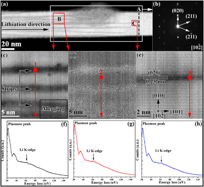
Figure 1 (a) HAADF image taken from the reaction front of a partially lithiated SnO2 nanowire. (b) The corresponding  zone axis SAED pattern taken from the area marked as A. (c and d) Higher magnification HAADF and the corresponding bright field images of the area marked as B in (a) showing the lithiation strips along the SnO2 nanowire, respectively. (e) An atomic resolution HAADF image taken from the area near the tip of one lithiation strip. (f)-(h) EELS spectra taken from the different areas (marked by red spots as 1, 2, 3 in STEM images (c-e) showing Li-K edge in the SnO2nanowire, respectively.
We also presented the results of this work in three international conferences including XXII International Materials Research Congress (IMRC), Aug 11-15, 2013, Cancun, Mexico; R. The 8th Pacific Rim International Conference on Advanced Materials and Processing, August 4-9, 2013, Waikoloa, Hawaii; and 245th American Chemical Society Meeting and Exposition, April 7-11, 2013, New Orleans, LA.