Reports: DNI1051456-DNI10: Novel Thermoelectric Material: Spin Seebeck Insulators
 printer friendly
1. Magnetism of side-wall epitaxial graphene nanoribbons
Introduction:
The past twenty
years have seen a tremendous upsurge of interest in magnetic materials, in
particular, in using the spin states in magnetic materials in novel information
storage and magnetic sensing devices [1]. Magnetic tunnel junction (MTJ) is an
unambiguous example of such devices (namely spintronics); it has been used as
the read-head of hard drive and also in the non-volatile magnetoresistive
random-access memory (MRAM). Tunnel magnetoresistance (TMR) of a MTJ device
consisting of two ferromagnets separated by a thin insulator exhibits
characteristic switch between two states of tunneling resistance, as the
magnetization direction of one of the ferromagnets is flipped. The relative
resistance change in TMR can be simply described as ![]() [2], where P1
and P2 are the spin polarizations of the two ferromagnets,
respectively. Therefore, studying the TMR of a MTJ between a known material
(which is Co in our case) and an unknown material (which is graphene nanoribbon,
GNR) can probe the edge magnetism of the ribbon and determine its spin
polarization.
[2], where P1
and P2 are the spin polarizations of the two ferromagnets,
respectively. Therefore, studying the TMR of a MTJ between a known material
(which is Co in our case) and an unknown material (which is graphene nanoribbon,
GNR) can probe the edge magnetism of the ribbon and determine its spin
polarization.
Tunnel magnetoresistance of graphene-nanoribbon-based magnetic tunnel junctions
It has been demonstrated recently that high-quality epitaxial GNRs can be reproducibly grown on the side-walls of both the 0001 and 000-1 faces of 4H and 6H SiC [3]. Surface sensitive measurements show that by controlling the growth conditions, the GNRs can be seamlessly connected to an insulating “buffer” layer [4], while electronic transport measurements demonstrate single-channel ballistic transport with both the spin and valley degeneracies lifted even at room temperature [5]. These observations signify the presence of spin-polarized edge states in GNRs.

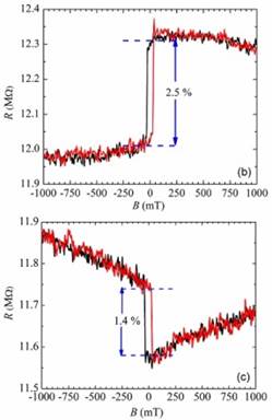
The magnetic properties of side-wall epitaxial GNRs can be further evidenced in the TMR measurements of Co–Al2O3–GNR MTJ junctions. Figure (a) illustrates the schematic of our measurement, where a 60 nm wide GNR was epitaxially grown on a pre-patterned side-wall and a 20 nm thick, 350 nm wide Co electrode was fabricated via e-beam lithography. In order to enhance spin ejection, a ~4 Å thick Al2O3 tunneling barrier was deposited on the GNR surface before the deposition of Co; several Au electrodes are also patterned across the GNR for characterization purposes with relatively transparent interface. The TMR is then measured using three-terminal configuration, as shown in Fig. (a). Figures (b) and (c) present our main results measured at 6.6 K for two different bias voltages, 24 mV and –27 mV, applied on the Co electrode. Interestingly, we observe a well-defined hysteretic loop around zero magnetic field: two abrupt switches in TMR appear at +/-23 mT, corresponding to the coercive field of the Co electrode. Note that both the resistance value of the TMR and the amplitude of the relative resistance change in Figs. (b) and (c) are much greater than the resistance of the Co electrode, therefore, the observed hysteresis loop is unlikely due to formation of magnetic domains in Co, but rather because the GNR itself is magnetic. The largest relative resistance change we have observed is ~9% (not shown). Assuming nearly perfect spin polarization of 34% for the Co electrode, we obtain >14% spin polarization in our GNRs.
Another striking observation in our measurements of Co–Al2O3–GNR MTJs is the switch of the sign in TMR, when the applied DC bias voltage changes the sign. This behavior can be clearly seen in Figs. (b) and (c), where the high resistance state is on the positive magnetic field side of Fig. (b) but on the negative side of Fig. (c). This observation suggests that Rashba effect may play an important role in polarizing the spins in GNR; the required electric field might be attributed to the charge transfer between the carbon atoms on the edge of GNR and the Si atoms of the SiC substrate. The rich physics embedded in the edge state magnetism of GNR invites further experimental and theoretical investigations. We are currently focusing on the spin Seebeck effect in GNR devices.
2. Impacts of the PRF project to the participating postdoctoral fellow, graduate student, and the PI
The postdoctoral fellow and the graduate student working on this project have learned a variety of experimental techniques and data analysis skills in characterizing the electronic and spin properties of GNRs. These techniques include ultrasensitive low-temperature transport measurements, photo- and electron-beam-lithography, metallic thin-film deposition and lift-off, etc. The experience gained in this project will benefit them in their future career in basic science or private industry. The experimental setups developed in this project have also benefited the PI in several other areas of research [6]. In particular, the low-temperature transport measurement setup has become to the most productive platform in the PI's lab, heavily used by all group members.
References:
[1] “Nobel Lecture: Origin, Development, and Future of Spintronics,” A. Fert, Rev. Mod. Phys. 80, 1517 (2008).
[2] “Tunneling between Ferromagnetic Films,” M. Julliere, Physics Letters A 54, 225 (1975).
[3] “Scalable templated growth of graphene nanoribbons on SiC,” M. Sprinkle, M. Ruan, X. Wu, Y. Hu, M. Rubio-Roy, J. Hankinson, N. K. B. Madiomanana, C. Berger, and W. A. de Heer, Nat. Nanotechnol. 5, 727 (2010).
[4] “A wide band gap metal-semiconductor-metal nanostructure made entirely from graphene,” J. Hicks, A. Tejeda, A. Taleb-Ibrahimi, M. S. Nevius, F. Wang, K. Shepperd, J. Palmer, F. Bertran, P. Le Fèvre, J. Kunc, W. A. de Heer, C. Berger, and E. H. Conrad, Nat. Phys. 9 49 (2013).
[5] “Exceptional ballistic transport in epitaxial graphene nanoribbons,” J. Baringhaus, M. Ruan, F. Edler, A. Tejeda, M. Sicot, A. Taleb-Ibrahimi, Z. Jiang, E.H. Conrad, C. Berger, C. Tegenkamp, and W.A. de Heer, arXiv:1301.5354.
[6] “Point-contact Andreev reflection spectroscopy of candidate topological superconductor Cu0.25Bi2Se3," X. Chen, C. Huan, Y. S. Hor, C. A. R. Sá de Melo, and Z. Jiang, arXiv:1210.6054.