Reports: DNI551339-DNI5: Surface Enhanced Raman Spectroscopy of Group IV Semiconductor Electrodeposition and Deoxygenation
 printer friendly
OVERVIEW. The goal of this project is to develop a simple and direct process that produces reduced covalent Group IV semiconductors in crystalline form through electrochemical methods. We employ a suite of material and surface analytical methods to characterize targeted electrodeposition strategies.
WORK DESCRIPTION. The original focus of the project was to study the preparation of Ge from GeO2 on Au substrates that support surface-enhanced Raman spectroscopy. The premise was that an in-situ vibrational spectroscopic probe would be informative on the initial bond-breaking and bond-forming processes in the deoxygenation process. However, during our investigations we serendipitously discovered that substitution of Au with a liquid metal electrode (e.g. Hg) dramatically impacted the product of the electrodeposition process. The liquid metal not only fully reduced the oxide but it facilitated simultaneously crystallization. In effect, we identified a new method for producing crystalline Group IV semiconductor materials that combined aspects of conventional electrodeposition and melt crystal growth. We have since described this process as an electrochemical liquid-liquid-solid (ec-LLS) crystal growth (Figure 1).
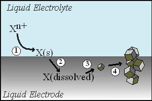
Figure 1. A schematic depiction of ec-LLS crystal growth. (1) Electrochemical reduction of a dissolved precursor in solution at the surface of a liquid metal electrode. (2) The dissolution of the electroreduced material (i.e. X) into the liquid metal electrode. (3) The spontaneous phase separation of X out of the liquid metal at a critical supersaturation concentration. (4) The subsequent crystal growth and precipitation of X.
We have previously described the initial findings and demonstrated ec-LLS as a means to make both crystalline materials AND device components (e.g. battery anodes) in one step. Through the support provided by ACS, we have been able to rapidly mature our understanding and control over ec-LLS processes. Specifically, we have achieved two landmark feats with regards to non-energy intensive syntheses of crystalline covalent semiconductors. First, we electrochemically produced crystalline Si in a single step at a record low temperature. Second, we demonstrated the possibility of electrodepositing single-crystalline Ge nanowires with epitaxy at room temperature from an aqueous bath.
ACHIEVEMENTS.
(1) With the goal of producing inexpensive crystalline Si, we recently reported the facile preparation of crystalline silicon films through direct electroreduction of dissolved SiCl4 in propylene carbonate at liquid gallium (Ga(l)) electrodes. In this system, we demonstrated ec-LLS for crystalline Si was possible and yielded crystalline Si at record low temperatures (T ≤ 100 °C, Figure 2). These results substantially bested the previous reported record for direct electrodeposition of crystalline Si (745 °C in a fluoride melt electrolyte) both in terms of energy input and simplicity. Our work is the first to show that a liquid metal can simultaneously operate both as an electron source for electrochemical reductions and as a separate phase for crystal growth for the preparation of crystalline silicon. The net conclusion was that ec-LLS may be a useful tactic for the preparation of Si-based optoelectronic technologies that can circumvent the enormous energy and environmental costs of current industrial practices for Si. We are presently working on extending this idea using dissolved SiO2 as the feedstock instead of SiCl4. In this capacity, we are motivated to show the feasibility of a direct “sand to silicon” process that can be performed under extremely benign conditions.
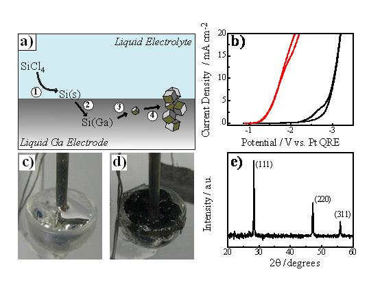
Figure 2. a) Schematic depiction of an electrochemical liquid-liquid-solid (ec-LLS) process yielding crystalline Si with a liquid Ga electrode (not drawn to scale). b) Voltammetric response for a liquid Ga electrode in propylene carbonate containing 0.2 M tetrabutylammonium and 0.5 M SiCl4. c) Optical photograph of a clean liquid Ga working electrode. d) Optical photograph of the same electrode after galvanostatic electrodeposition of Si at 100 oC. e) Representative X-ray diffractogram collected with the black film in (d).
(2) We recently described an ec-LLS method for the epitaxial growth of single crystalline, covalent group IV semiconductor nanowire films that can be performed with an aqueous solution at room temperature (Figure 3). Using liquid Ga nanodroplets on crystalline substrates, we showed direct electrodeposition of single crystalline Ge nanowires with either homo- or heteroepitaxy. The method is general and scalable, yielding standing Ge nanowire films over the surface of an entire wafer (> 10 cm2). The salient features of our method are that it requires no expensive thermal/vacuum equipment, inexpensive and unrefined starting chemicals, and can be performed with electrolytes nearly identical to those already used in the semiconductor industry for metallization.
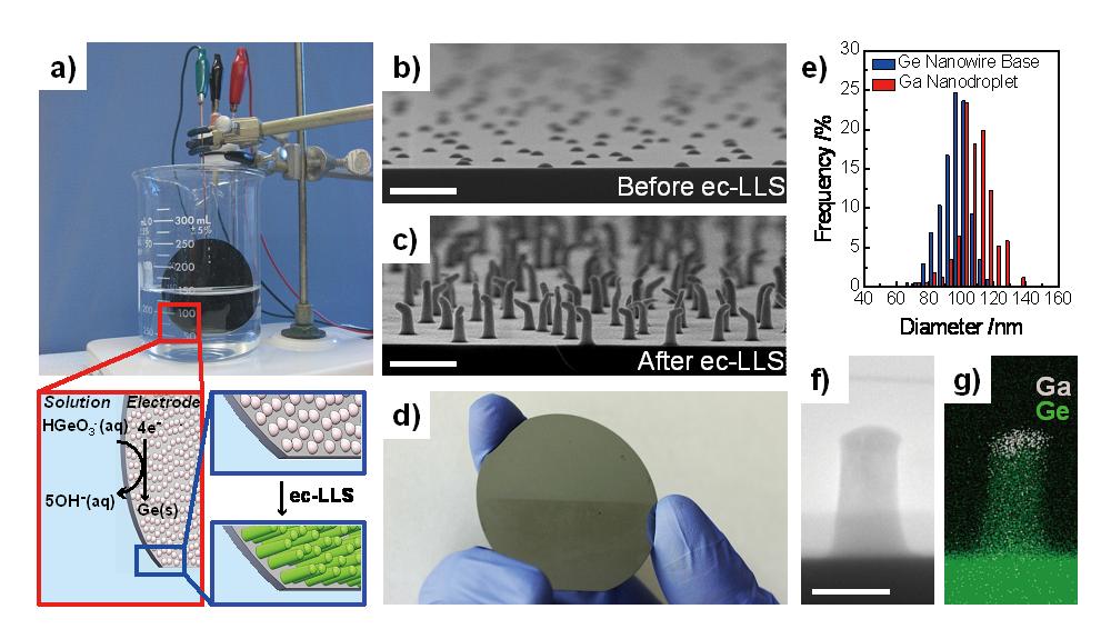
Figure 3. a) The benchtop experimental setup used for wafer-scale ec-LLS of Ge nanowire films. Insets: Schematic depiction of ec-LLS process. b) A cross-sectional scanning electron micrographs of a Ge(111) substrate decorated with discrete liquid Ga nanodroplets. c) Same as (b) but after 60 s ec-LLS process. Scale bar: 500 nm. d) Optical image of a 2-inch wafer coated with Ge nanowires after 300 s ec-LLS nanowire deposition over the bottom half of the wafer. e) Size distribution of the Ga nanodroplet electrodes and resultant Ge nanowire base widths obtained after a 30 s ec-LLS experiment. f) Cross-sectional high resolution transmission electron micrograph of an as-prepared single Ge nanowire on a wafer substrate produced after a 30 s ec-LLS. g) Energy dispersive X-ray map of the elemental map of the structure in (f). Scale bar: 100 nm.
IMPACT OF FUNDS. The support of the ACS PRF program has enormously augmented my research program. Through the ACS PRF program, my group has advanced an innovative project that was outside of what my start-up funds could support. This work undoubtedly has become my group's greatest achievement to date and has shaped the focus of my career moving forward. As of this writing, we have published three high profile publications on the ec-LLS method, with another manuscript submitted to Nature Materials. In addition, data for another three manuscripts has been collected and are in the preparation stages for peer-reviewed submission. This work has allowed me to attract several high quality students that specifically want to work on ec-LLS based projects. In addition, I have made collaborative partnerships in the energy and electronics industries (e.g. Nissan, IBM) based on this work.