Reports: ND1051514-ND10: Designing Novel Organic/Inorganic Hybrid Architectures for Efficient Energy Conversion
 printer friendly
The objective of this project was to explore new approaches to organic/ inorganic hybrid photovoltaic architectures. Focus thereby was to gain fundamental understanding of the electronic and optical processes occurring at organic/ inorganic interfaces. This required fabrication of well-defined structures and interfaces both of the inorganic and organic components. Hence, in the first part of the project, we concentrated on the design and fabrication of well-defined inorganic structures based on ZnO. For comparison we prepared bi-layers, mesoporous architectures to ordered nanostructures in close collaboration with one of the main project partners (Dr. Martyn McLachlan, Imperial College London). In the second year of the project we focused on the organic component and investigated how the physical organization, from the molecular to the macro-scale can be controlled. We followed a strategy often used in the bulk commodity plastic field: i.e. controlling nucleation of the organic material from the liquid state by use of nucleating agents.
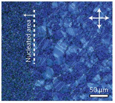
Fig. 1. Beneficial features of using nucleation agents in combination with organic semiconductors as demonstrated by the surface nucleation of PCBM from evaporated DMDBS patterns deposited on a glass surface (line width of 150 m).
We studied nucleating agents as this class of additives have commonly been used in the commodity ‘plastic' field to manipulate the solidification process of (semi-)crystalline polymer solids and other organic matter. Using this approach, we found that minute amounts (0.1 – 1 wt%) of such commercially available nucleating agents can also be used to efficiently manipulate the solidification kinetics of a wide range of organic semiconductors —including poly(3-alkylthiophene)s, the fullerene derivative [6,6]-phenyl-C61-butyric acid methyl ester (PCBM) and 6,13-bis(triisopropyl-silylethynyl) (TIPS) pentacene— when processed from the melt, solution or solid state, without adversely affecting the semiconductors' electronic properties. This should have strong implications on organic/inorganic hybrid fabrication as this reduces the dependency of film formation on the chemical nature of the inorganic template. Moreover, our work shows that heterogeneous nucleation increases the temperature and rate of crystallization of the organic materials. This was demonstrated with poly(3-alkylthiophene)s. Moreover, use of nucleating agents permits patterning of crystallites at pre-defined locations when using the fullerene PCBM (Figure 1). Also, we found that these additives minimize dewetting of films of TIPS-pentacene from surface-treated SiO2.This is best illustrated by the wetting behaviour of inkjet-printed TIPS-pentacene films (Figure 2). Films deposited from solutions comprising no nucleation agent only grew on the gold electrodes but not in the channels between them. In stark contrast, heterogeneous nucleation through use of our additives allowed continuous films to be printed covering both the gold and SiO2 surfaces. As a consequence, addition of a ‘dash' of nucleation agent resulted in a drastic improvement in the number of working devices from 0% to 100% -highlighting the technologically highly beneficial aspect of our approach not only in the field of organic/inorganic hybrids.
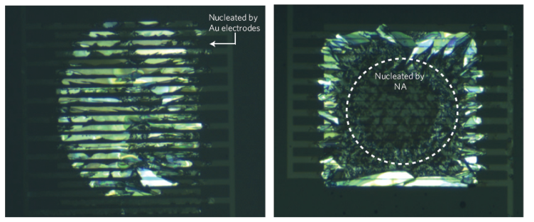
Fig. 2. Use of nucleation agents reduces undesirable dewetting effects during inkjet printing of small-molecule semiconducting inks. The crossed-polarized optical micrographs (height: 660 mm and width: 820 mm) show an inkjet-printed drop onto an OFET substrate with a dielectric treated with octadecyltrichlorosilane (OTS): ink comprising no nucleation agent (left); ink comprising a minute amount of DMDBS (right).
Moreover, we used the support supplied by the ACS Petroleum Research Fund for educational projects for under- and postgraduate students (MSc, MRes, PhDs) as well as postdoctoral researchers. The Chemistry undergrad student Alise Virbule, for instance, spent three months during the summer of 2013 in our labs working on the patterning of organic/ inorganic hybrid structures. She was educated in polymer surface structuring methodologies such as embossing and micromolding in capillaries (MIMIC) and applied this to organic/ inorganic systems. Initial experiments to fill the structures with the polymer semiconductor P3HT have also been made. Another undergraduate student, Annie Rumbles, started an outreach project in the area enhancing the web-presence of our research using, among other tools, Wikipedia. PhD-students and postdocs, including Paul Westacott and Drs. Christoph Hellman and Neil Treat, spent time for field work experiments at partner institutions. At the National Renewable Energy Laboratory at Golden, CO, Dr Neil Treat was, e.g., exposed to how to conduct microwave conductivity experiments assessing how nucleation agents affect the electronic properties of the organic semiconductors. Overall, various new collaborations could be established in this way during the course of the project, and young people were attracted to Chemical Sciences.