AmericanChemicalSociety.com
Reports: AC5 47304-AC5: Structures and Defects at Interfaces in Organic Molecular Heterostructures
Organic/inorganic semiconductor interfaces have an important role in emerging electronic materials for application in organic light emitters and in organic photovoltaic solar energy harvesting. Despite much work on these devices, there are many challenges that must be surmounted, most importantly the need to understand and control the electronic properties. The creation of novel interfaces, including those based on new molecular-scale structures or new materials, leads to the opportunity to bring new functions to organic devices. We have used scanning tunneling microscopy techniques to probe how organic/inorganic semiconductor interfaces are formed and to characterize their structure and electronic properties. We have made significant progress in understanding the structure and electronic properties of a prototypical organic semiconductor/inorganic semiconductor interface consisting of a junction between pentacene and the nitrobenezene-terminated surface of silicon. This interface is an example of the precise structures that can now be created in organic/inorganic systems, chosen because it is an excellent demonstration of the role of an interface molecule in determining the electronic properties of the junction. Section 1 below describes a test of theoretical predictions of the structure of this interface a study of its electronic properties. Section 2 describes the use of similar organic thin film growth techniques to produce thin films of an organic ferroelectric material, which will allow us to expand the range of properties that can be used to control the flow of charge at these interfaces.
1. Structure and electronic properties of the pentacene-nitrobenzene-silicon interface
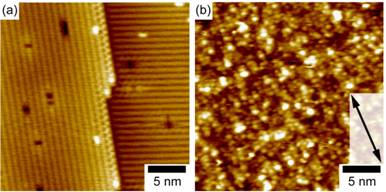
The properties of organic/inorganic interfaces depend sensitively on their composition and structure. In order to create a prototypical interface from the ground up, we have developed an interface between the organic semiconductor pentacene and silicon in which a monolayer of the molecule nitrobenzene is located at the interface. By doing this we have created a system in which the effects of the electronic properties of the intervening molecular layer can be precisely studied. The process of creating this interface begins with the clean (001)-oriented silicon surface, which has an extremely well defined composition and structure, as shown in the ultrahigh vacuum scanning tunneling microscopy (STM) image in Fig. 1(a). The surface is then exposed to nitrobenzene under ultrahigh vacuum conditions which forms a single-layer of reacted molecules. A simultaneous theoretical study of the structure of nitrobenzene molecules attached to Si was conducted in collaboration with the research group of Prof. Manos Mavrikakis (UW-Madison). By comparing theory and experiment, we have found that the disordered structure evident in the nitrobenzene/Si surface in Fig. 1(b) results from an incomplete conversion of the system to the lowest-energy configuration from the state reached by the initial attachment of the molecules.
Fig. 1 Formation of the Si
(001)/nitrobenzene interface. (a) STM image of the reconstructed Si (001) 2 x 1 surface starting
point. (b) STM image of the
surface after attachment of the nitrobenzene molecular layer.
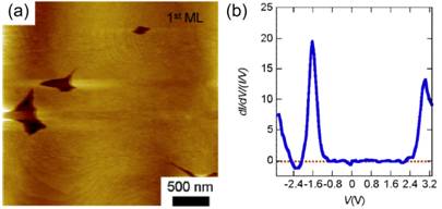
A molecular pentacene/nitrobenzene/Si junction is then
created by depositing pentacene onto nitrobenzene-terminated Si surface. The chemical attachment of nitrobenzene to
the surface leads to an unreactive interface on which
pentacene forms large smooth crystals, as shown in Fig. 2(a).
Fig. 2 (a) STM image of a the
surface of a pentacene thin film grown on the nitrobenzene/Si surface. (b) Scanning tunneling spectroscopy
measurement of the normalized differential conductance dI/dV/(I/V) of the pentacene/nitrobenzene/Si junction,
measured using the current flowing through the junction (I) and voltage (V)
applied across it..
The electronic properties of the
pentacene/nitrobenzene/silicon system can be probed using current voltage
characteristics measured using scanning tunneling spectroscopy (STS). The results of an STS measurement of the
derivative of the current with respect to the current are shown in Fig. 2(b). The derivative is normalized with respect to
the total current in order to allow features at higher voltages to be
seen. The strong peak in the derivative
of the current at -1.6 V in Fig. 2(b) results from negative differential
resistance in this structure. From this
effect, we know that the nitrobenzene layer between the pentacene and silicon
impedes the flow of charge and leads to resonant tunneling between the tip and
the interface. The existence of a strong
barrier between pentacene and nitrobenzene provides insight into the design of
monolayers that will allow charge to flow easily between organic and inorganic
phases.
2. Organic ferroelectric thin film growth
The wide range of properties available in organic molecular
materials presents a wide range of opportunities to tailor the electronic
properties of interfaces. We have
expanded the range of materials available as organic thin film materials by
developing a process that allows us to deposit thin films of a molecular
organic ferroelectric material.
Ferroelectrics have a large permanent electric dipole moment, termed the
remnant polarization. By including this
dipole moment at an interface it will be possible to modify the alignment of
electronic states across the interface or to induce a permanent charge density
in a subsequently grown semiconducting layer.
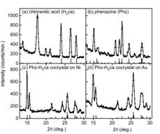
We have grown thin films of a prototypical organic ferroelectric
material consisting of a cocrystal of the molecules phenazine and chloranilic
acid. The layers we produce have x-ray
diffraction patterns indicative of the formation of the cocrystal on both Ni
and Au, and which are clearly distinct from the diffraction patterns of the
components (Fig. 3). The ability to grow
these layers provides the basis for using permanent ferroelectric dipole
moments as an additional degree of freedom in manipulating the electronic
properties of organic/inorganic semiconductor interfaces.
Fig. 3 X-ray diffraction q-2q scans with Cu Ka
radiation for thin films of (a) chloranilic acid (H2ca), (b)
phenazine (Phz), and a Phz-H2ca cocrystal
on (c) Au and (d) Ni bottom electrodes.
Angles associated with reflections of the reported structure of each
material are represented as vertical lines with heights proportional to the
intensity reported in powder diffraction studies. Reflections for both polymorphs of phenazine
are shown in (b).