AmericanChemicalSociety.com
Reports: B10 48489-B10: Photonic Crystals-based Hybrid Structures for Laser and Photovoltaic Applications
In order to realize our final goal of making structures suitable for laser and photovoltaic applications, we undertook two major projects during the past year. In the first project, since we had comprehensively categorized the TiO2 nano-structures using Raman spectroscopy, as reported in our previous year's report, we wanted to address the specific issue of index of refraction variance with porosity and pore diameter of mesoporous TiO2. Extending this study to SiO2 mesoporous films, we were able to build a library of constituents suitable to build the alternate layers in a Bragg-mirror structure. This project has enabled us to understand the issues related to mirrors, which is one of the components of the structures we plan to fabricate. In the second project, we investigated, especially the growth-related issues, on how to incorporate a thin film between two 3-D photonic crystals.
A. Dielectric Mirrors of TiO2 and SiO2
In both types of mesoporous films related to TiO2 and SiO2, we have observed that the index of refraction varies with respect to the porosity. This has enabled us to fabricate an array of films with various porosities. After growing individual films of each type and understanding their behavior, we tried to grow multiple stacks of TiO2 and SiO2. We encountered several growth related problems while fabricating these monolithic structures. Since each layer is embedded with pores, while spinning the subsequent layer on top of another, the top-layer solution tends to infiltrate into the pores. This alters the index of refraction of the bottom layer and reduces the overall reflectivity of the final structure. In order to get moderate reflectivity values, through calculations, we have determined that at least 6 periods of TiO2 and SiO2 are needed. In our last year's report, we showed a structure with 3 periods. Although we were able to get several structures with that many periods, it has been very difficult to extend the number of periods in such way that our results are reproducible. The major impediment of solution infiltration into the bottom layers has resulted in structures with unpredictable indices of refraction.
B. Hybrid Structures
In the proposed work, we plan to use photonic crystals as mirrors in laser and photovoltaic devices. We fabricated photonic crystals using SiO2 spheres, which were assembled by using a technique called evaporation-based self-assembly. In the past year, we have optimized this technique, solving several issues related to their growth. In Fig. 1a, we show a reflectivity spectrum of a photonic crystal fabricate using SiO2 spheres of around 250 nm reflectivity band corresponds to the wavelengths rejected by the photonic crystal. In other words, these frequencies are in the forbidden gap of the structure. In addition to the high-reflectivity band, we also see the many lobes at higher wavelengths, suggesting the uniformity of the photonic crystal. Encouraged by this work, we then began constructing monolithic structures where a thin film of SiO2 mesoporous layer is embedded between two photonic crystals.
The reason to grow such structures is to obtain a microcavity-like device in which the cavity modes are exploited. Similar to the doping process in semiconductors, the incorporation of the mesoporous film between the photonic crystals, introduces defect-like states in the original band structure of the photonic crystals. The cavity which acts like a defect, allows one to access states in the forbidden range, resulting in the propagation of forbidden frequencies through the material. This is shown in Fig. 1b, where a dip in the reflectivity signifies the transmission of light corresponding to that particular wavelength which was previously forbidden by the original photonic crystal.
The fabrication technique used to form the cavity-based photonic crystals consisted of several steps. After assembling the silica-based photonic crystal on a glass slide, the mesoporous layer was subsequently spin-coated on top of the bottom photonic crystal. Prior to this procedure, we infiltrated a sacrificial material into the bottom photonic crystal to avoid the mesoporous solution infiltrating into the photonic crystal during spin-coating. Finally, the top photonic crystal was fabricated.
Next we tried to exploit the defect state of the photonic crystal by infiltrating a chemical into the pores of the defect state. It must be noted that the dip in the reflectivity spectrum, corresponding to the defect state, is entirely dictated by the index of refraction and the thickness of the mesoporous layer, or in other words, the cavity between the two photonic crystals that act like mirrors. Exploiting on the porous structure of the cavity, we probed the dynamics of the cavity peak as a function of the infiltrated dose of a chemical called TMOS. As the chemical infiltrates the pores, the index of refraction is changed and subsequently, the position of the dip in the reflectivity spectrum changes accordingly. As shown in Fig. 1b, we observed that the defect peak red shifts by about 15 nm as we introduce doses of TMOS into the structure.
In the final year of our project, we will concentrate on incorporating quantum dots into the defect layers. If we can place the emission of the quantum dots to coincident with the cavity peak, then we can modify the emission of the quantum dots. This will enable us to study the cavity dynamics associated with these monolithic structures, and allow us to build interesting devices suited for lasers and photovoltaic dapplications.
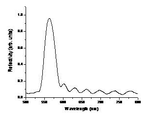
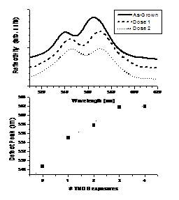
Figure 1: (a) Reflectivity spectrum of a photonic crystal fabricated using silica spehers. (b) Evalution of the cavity peak as TMOS infiltrates the mesoporous layer sandwhiched between two photonic crystals.
