AmericanChemicalSociety.com
Reports: DNI10 49952-DNI10: Photocarrier Generation and Multiplication in Carbon Nanotubes
Summary
During the first year of funding we have built a scanning photocurrent microscope (SPCM) suitable for addressing pn junctions built from individual single-walled carbon nanotubes (CNTs). We tested the operation of this microscope using a basic CNT device structure. In parallel, we have demonstrated the feasibility embedding CNTs in dielectrics for the proposed experiments. During the upcoming year we plan to investigate changes in the quantum efficiency of photocurrent generation as we tune the environment of CNT pn junctions.
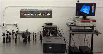
Figure 1 Caption: Photograph of the new scanning
photocurrent microscope. Spatial resolution of the
SPCM SPCM
images are obtained by focusing a light source to a submicron spot and raster
scanning across a photosensitive device. Photocurrent is mapped as a function
of position. The photocurrent is driven by built-in electric fields. These fields are caused by chemical and/or electrostatic doping of
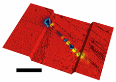
the CNT. Figure 2 shows one of our first SPCM images. The CNT device is
fabricated on an oxide surface. There are hot spots along the length of the CNT
where positive/negative current is generated. The current direction is
determined by local electric fields. In this device the electric fields are uncontrolled
- they are caused by either the oxide surface or by defects in the CNT. In
future devices we will minimize uncontrolled electric fields by suspending the
CNT above the surface and using local gates to induce p-type and n-type doping (see
device fabrication below).
Figure 2 Caption: Scanning
photocurrent data overlayed on an AFM height image.
Scale bar 5 microns. The height image shows a pair of metal electrodes (30 nm
tall) and a single CNT bridging the gap between the electrodes. The color scale
shows photocurrent as a function of laser position: Negative current (blue),
zero current (red), positive current (yellow). Spectral resolution of the
SPCM The
light source for our SPCM is a super continuum laser. This light source outputs
a spectral power density > 1 mW/nm over a broad range
of wavelengths (450 nm – 2000 nm). We select a narrow bandwidth (~ 2 nm)
using a computer-controlled monochromator. Our
optical components are currently optimized for visible and near IR, limiting
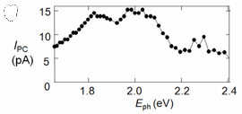
the practical wavelength range to 450 – 800 nm. Figure 3 shows the spectrally-resolved
photocurrent response from the Schottky barrier of a 4
nm diameter CNT. The peaks in photocurrent likely correspond to resonant
absorption peaks of the CNT. For future work we will work with CNTs with smaller diameters. Previous work by others has
shown that significantly sharper resonant absorption peaks can be expected. The
quantum efficiency of photocurrent generation at these absorption resonances will
be the subject our future work.
Figure 3 Caption: Normalized photocurrent
(normalized with respect to incident light intensity) as a function of photon
energy. The light source is focused on the Schottky
barrier of a CNT device. Photocurrent values correspond to a light intensity of
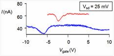
approximately 3 x 10^7 W/m^2. Device fabrication We
have fabricated devices by growing CNTs on Si/SiO2 substrates. We then deposit
a pair of metal electrodes onto the ends of the CNT. On some devices we have
tested dielectric coatings that are expected to significantly change the
properties of the CNT. Figure 4 shows the electrical characteristics of a
device before and after the deposition of aluminum oxide (10 nm thickness)
using atomic layer deposition. There is a small change in doping level
(horizontal shift on the V_gate axis). There is also
a change in contact resistance. These changes are acceptable and will not pose
any problems for comparative measurements of the efficiency of photocurrent
generation.
Figure 4 Caption: Electrical characteristics
of a small-bandgap CNT device before (red) and after (blue) a 10nm Al2O3
coating. After application of Al2O3, the CNT was doped more n-type and contact
resistance was increased by about 30%. For
future devices we aim to control the built-in electric field in the CNT. The
CNTs will be suspended above the oxide surface. A pair of gate electrodes on
the oxide surface will electrostatically dope the CNT
to form a pn junction. We plan to fabricate these new devices at the Cornell
Nanofabrication Facility (CNF) where we have access to etching tools and high-resolution
photolithography. Impact on career Preliminary
data taken from the SPCM microscope was the foundation for the PI's NSF CAREER award application (submitted July 2010). The
SPCM has also given the PI's lab a unique advantage
in the field of nanometrology. This new nanometrology tool has lead to collaborations with Prof. Oksana Ostroverkhova (OSU), Prof.
George Nazin (UO) and Prof. Paul McEuen
(Cornell University). Impact on students Tristan
DeBorde (PhD candidate at OSU, Physics) and Rachel
Burton (undergraduate physics major at OSU) have been supported by the research
funds. Tristan began working on the project in Jan 2010. Over the last 9 months
he has become an expert in SPCM. He is also becoming familiar with the cutting
edge questions in CNT opto-electronics research.
Rachel has become an expert in chemical vapor deposition growth of CNTs. As a summer student she has provided Tristan and other members of
the research group with high quality single walled CNTs which we are currently
making into device. Feedback from Rachel confirms that the research
experience has been both exciting and motivational.