AmericanChemicalSociety.com
Reports: UFS 49376-UFS: Imaging band bending in photovoltaic devices using scanning electron and scanning probe microscopy techniques
During my 2009-2010 sabbatical at the National Renewable Energy Laboratory (Golden, Colorado), I developed collaborations with Dr. Mowafak Al-Jassim, Dr. Chun-Sheng Jiang, and other colleagues within the measurements and characterization group of the National Center for Photovoltaics. There, my knowledge of photovoltaic materials characterization increased dramatically, particularly in the realm of probe microscopy and electron microscopy techniques. Our work has been highly productive, and I look forward to following up on several of our initial studies with my students at Linfield College.
This experience expands my vision of research possible in my own lab and with collaborators. In accordance with the proposal's goals, I expect within the next year to solicit grants to improve the teaching and research laboratories at Linfield. In fall 2010, I will recruit physics students to help model and interpret some of the experimental data collected during this sabbatical.
During the sabbatical, I was able to give presentations on this work at the American Physical Society (APS) March Meeting (2010), New Mexico Institute of Technology physics colloquium (April 2010), Materials Research Society Spring Meeting (April 2010) , and IEEE Photovoltaic Specialists Conference (June 2010). The latter two presentations include publications in peer-reviewed conference proceedings, both in press. I also completed a book chapter coauthored with P. Zabierowski for Characterization Techniques for Thin-Film Solar Cells, edited by D. Abou-Ras, T. Kirchartz, and U. Rau (Wiley, to be published spring 2011). Other publications are in preparation, and ongoing research continues. I will present in colloquia at Linfield College and Willamette University and in a plenary talk at the APS-Four Corners meeting this fall.
Our research focused on better understanding the origins of signal contrast observed in images of photovoltaic devices measured using Scanning Capacitance Microscopy (SCM) and Secondary Electron detection (SE) in the scanning electron microscope. We found that these techniques are capable of indicating both variations in potential (band-bending) and associated depletion regions in cross-sectioned photovoltaic devices. We studied images both near grain boundaries and p-n junction interfaces in cross-sectioned multicrystalline Silicon and GaAs devices.
It has been known for many years that p and n type materials can be qualitatively distinguished in SE images, with n type materials generally appearing darker. We found that for both multicrystalline Silicon devices with diffused (n+) emitters and for single or multijunction III-V devices, SE allows the metallurgical junction to be quantitatively located and the depletion region width to be imaged. These data also agreed with SCM and Scanning Kelvin Probe Microscopy results. Because the SE signal varies quadratically across the interface, in agreement with PC1D simulations of the expected band bending, a spatial derivative yields local maxima at metallurgical junctions. An example of such data is shown in Fig. 1. Such images are particularly valuable for textured devices. By observing the change in the SE image with applied dc bias across the device, our results contribute new information about the origin of the p-n contrast, which has been a topic of study for decades.
The SE technique, however, is not appropriate for studying electronic properties of grain boundaries because of the potentially large effects on the signal of grain boundary strain and the change in surface orientation. Instead, we found that SCM, when carefully implemented, was capable of imaging depletion regions near grain boundaries due to band bending. In SCM, the surface oxide is assumed to be of uniform thickness, and most data in the literature are
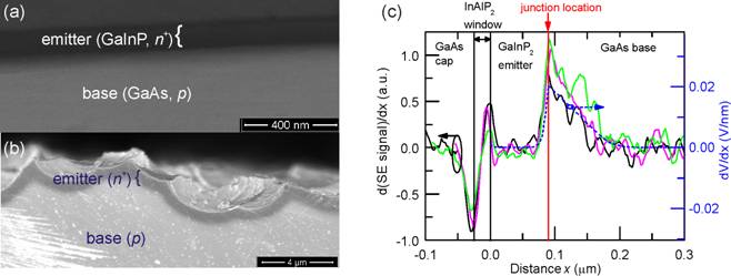
Fig. 1. (a) SE image of a cross-sectioned GaAs/GaInP heterojunction at a reverse bias of 0.0V.
(b) Textured multicrystalline Silicon photovoltaic device, showing a clear contrast between the n+ emitter (darker region) and p-type absorber materials. The uniformity of the n+ emitter can easily be observed.
(c) A spatial derivative of the SE data peaks at the metallurgical junction. These data are for the sample shown in (a), held at reverse bias of 0.0V (black line), 0.75V (magenta line), and 1.75V (green line). Results of a numerical model of the bulk band bending at 0.0V using PC1D (blue dashed line), and the known junction location (red line) are also shown. In this case, the junction location is known from the device deposition process.
collected on single crystalline materials; in our multicrystalline devices, the surface oxide likely varies for different grain surfaces or grain boundary orientations. We used the variation of the capacitance signal with applied dc bias to better distinguish surface from bulk effects, allowing the SCM images to be interpreted with a higher level of confidence. In the SCM images, we observed depletion regions near certain higher-order grain boundaries in multicrystalline silicon devices, but not on S3 twin grain boundaries (Fig. 2); the grain boundary orientations were identified by electron backscattering diffraction.
These studies allow SE and SCM images of p-n+ junctions, and SCM images of grain boundaries, to be more quantitatively understood; thus, these two imaging techniques can make a valuable contribution to our understanding of the electronic properties of low-cost photovoltaic materials.
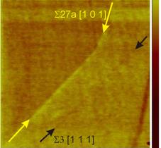
Fig. 2. 5mm SCM image including two grain boundaries. Orientation was identified by EBSD measurements. The S27a grain boundary consistently shows a depletion region, evident as a bright line in this image, while the S3 grain boundary does not.
