44259-AC5
Charge Transfer between Semiconducting Substrates and Organic Molecules
For XPS and UPS, substrates were prepared by first removing the oxide in a dilute HF (~1%) solution, followed by annealing to about 700 C. The surface reconstruction was confirmed by the presence of characteristic surface features. The molecules were purified by several freeze-pump-thaw cycles or by pumping directly, and the purity of the molecule was checked by RGA. Molecular exposures were measured in Langmuir, where 1 L = 10-6 Torr x 1s.
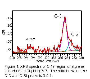
Bonding of phenylacetylene and styrene on Si (111) 7x7 was confirmed by XPS of the C 1s region (figure 1). Two features are evident in the spectra: the C 1s transition and a loss peak resulting from the p-p* shakeup. The C 1s transition can be decomposed into two components, one centered at 285 eV corresponding to C-C and C-H bonds from the styrene, and the lower binding energy component (~283.5 eV) corresponding to C-Si bonds. The ratio of the C-C to C-Si components is about 4:1, suggesting the molecules bind at two carbon sites. The presence of the p-p* shakeup suggests the styrene retains aromaticity after bonding on the silicon surface.
UPS measurements of the valence region of
silicon (111) 7x7, with increasing exposure to phenylacetylene and styrene,
show significant changes in valence band features. The
characteristic 7x7 surface features disappear after 10 L exposure
phenylacetylene and after just 2 L exposure styrene, showing the formation of a
saturated monolayer. New molecular features develop with increasing
exposure. These features show good agreement with the theoretical density of
states calculated by density functional theory. Extrapolating the start
of the valence features for the two molecules after 100 L exposure, the
molecular highest occupied molecular orbital is found to be at 0.7 eV below the
Fermi level for both molecules.
To measure unoccupied state information, STM measurements
have also been made on these systems. For STM, silicon 111 (7x7) surfaces
were prepared by flash-annealing to 1250 C. The molecules were dosed as describeed above. In occupied state images (negative
sample bias), both phenylacetylene and styrene appear as protrusions above the
silicon surface. In unoccupied state images, however, the styrene appears
as a depression, while phenylacetylene still appears as a protrusion –
showing that at the applied biases of 2 V, styrene has few or no molecular
states available for tunneling.
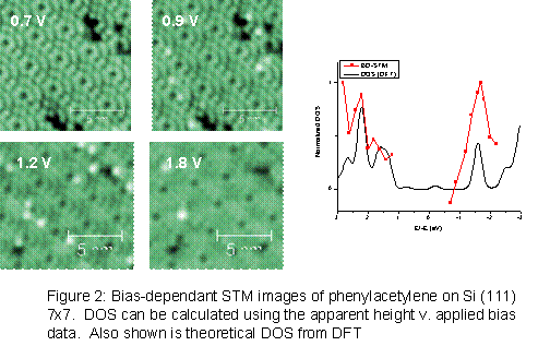
Bias dependent STM has also been performed on the
phenylacetylene/silicon systems (figure 2). Since the apparent height in
STM images is a convolution of physical height and electronic structure,
tracking the changes in apparent height of the molecule at various applied
biases will give an indication of the local electronic structure. The
onset of tunneling into the molecular states occurs between 0.7 and 0.9 V applied
sample bias. The phenylacetylene apparent height then increases with bias
until 1.6 V, after which it decreases to a level indistinguishable from the
silicon substrate. Calculating the density of states from the apparent
height data, the lowest unoccupied molecular orbital (LUMO) is found to lay
approximately 1.7 eV above the Fermi level, consistent with the density of
states calculated by density functional theory.
Using XPS, UPS and STM we have investigated the chemical and
physical interface of styrene and phenylacetylene adsorbed on silicon (111) 7x7
surfaces. XPS and UPS confirm the chemical attachment between molecule
and substrate. The HOMO of both molecules is seen to lay 0.7 eV below the
silicon Fermi level from UPS measurements; the LUMO of phenylacetylene is found
to be about 1.7 eV above the Fermi level, while that of styrene is greater than
2 eV above.
References:
(1) Linsday,
S. Journal of Chemical Education. 2005,
82, 727-733. (2) Haiss, W.; et al. Nature Materials. 2006,
5, 995-1002.