

45842-G5
Visualizing the Interplay Between Electronic Excitations and Surface Chemistry of the Functioning 1-D Metal-Oxide Nanostructures
Fig. 1 SPEM chemical mapping of the SnO2 nanowire on Au support at Au 4f and Sn 4d photoelectrons. Bottom: LEEM imaging and LEED pattern from the individual SnO2 nanobelt
|
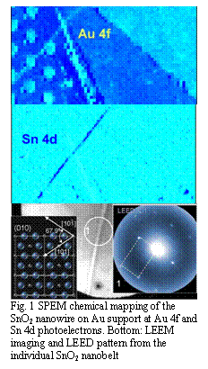
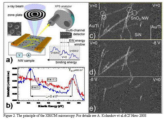
Figure 2. The principle of the XBICM microscopy. For details see A. Kolamkov et al ACS Nano 2008 |
 Understanding
size/dimensionality dependent phenomena and processes of relevance for chemical
sensing and catalysis by nanostructures require analytical methods with high
surface sensitivity, which can exploit the structure and composition of
nano-materials at their natural length scales and working conditions. In the
frame of the present ACS PRF-G granted research we explored the potentials and
complementary capabilities of several microscopy approaches in terms of
imaging, spatial resolution, structural and chemical sensitivity to shed light
on the properties of individual SnO2 nanowires and their networks. The obtained
results demonstrate the unique opportunities provided by synchrotron-based
photoelectron microscopies for structural and
chemical analysis, including in-situ electron transport properties
characterization of a nanostructure wired as an active element in chemiresistor
devices. In collaboration with Tulane University (Prof. U. Diebold) and ELETTRA
spectromicroscopy (Drs. M. Kiskinova and A. Locatelli)
groups, we have successfully applied an array of powerful spectromicroscopy
surface science tools such as X-Ray Photoemission Electron Microscope (X-PEEM),
Scanning Photoemission Microscope (SPEM) , Low-energy
electron microscope (LEEM) ( all at ELETTRA, Italy) and STM (performed at TU)
to individual metal oxide nanowires and nanobelts. The large scale STM images
of the top facets of SnO2 nanobelt reveal the morphology of the surface which
is dominated by wide terraces confined by atomic steps and voids. The
atomically resolved STM, for the first time obtained on oxide nanobelts,
confirm (101) structure of the exposed facets and were backed up with LEED
(1x1) pictures taken from the local areas along the length of the nanobelt
Fig.1. Local XPS, UPS and XANES spectra from the individual nanowires and
nanobelts indicate the similarity of the surface stoichiometry, coordination
and oxidation state of the nanostructures with respect to their macroscopic
counterparts. Being extremely important for screening effects, apparently 100
nm size domain is still too large to induce measurable
size effects.
Understanding
size/dimensionality dependent phenomena and processes of relevance for chemical
sensing and catalysis by nanostructures require analytical methods with high
surface sensitivity, which can exploit the structure and composition of
nano-materials at their natural length scales and working conditions. In the
frame of the present ACS PRF-G granted research we explored the potentials and
complementary capabilities of several microscopy approaches in terms of
imaging, spatial resolution, structural and chemical sensitivity to shed light
on the properties of individual SnO2 nanowires and their networks. The obtained
results demonstrate the unique opportunities provided by synchrotron-based
photoelectron microscopies for structural and
chemical analysis, including in-situ electron transport properties
characterization of a nanostructure wired as an active element in chemiresistor
devices. In collaboration with Tulane University (Prof. U. Diebold) and ELETTRA
spectromicroscopy (Drs. M. Kiskinova and A. Locatelli)
groups, we have successfully applied an array of powerful spectromicroscopy
surface science tools such as X-Ray Photoemission Electron Microscope (X-PEEM),
Scanning Photoemission Microscope (SPEM) , Low-energy
electron microscope (LEEM) ( all at ELETTRA, Italy) and STM (performed at TU)
to individual metal oxide nanowires and nanobelts. The large scale STM images
of the top facets of SnO2 nanobelt reveal the morphology of the surface which
is dominated by wide terraces confined by atomic steps and voids. The
atomically resolved STM, for the first time obtained on oxide nanobelts,
confirm (101) structure of the exposed facets and were backed up with LEED
(1x1) pictures taken from the local areas along the length of the nanobelt
Fig.1. Local XPS, UPS and XANES spectra from the individual nanowires and
nanobelts indicate the similarity of the surface stoichiometry, coordination
and oxidation state of the nanostructures with respect to their macroscopic
counterparts. Being extremely important for screening effects, apparently 100
nm size domain is still too large to induce measurable
size effects. In analogy with EBIC imaging mode in traditional scanning electron microscopy we have developed a new X-Ray Beam Induced Current Microscopy (XBICM). XBICM was tested via application of the SPEM to the working chemiresistor device composed of mats of the percolating nanowires Fig.2. Imaging the potential distribution along the biased percolating network of nanowires with XBICM, we revealed the presence of “electro active “elements which controls the transport trough entire percolating path. This approach opens new avenues to explore the very surface structural and electronic properties of the individual nanostructures as a function of nanostructure size, morphology, type of adsorbate, temperature. In addition we showed that the method is applicable to the nanostructures wired as an active element of the functioning nanodevice (chemiresistor in our case). The latter offers the unique experimental platform to link fundamental surface processes taking place on the nanowire surface and its electronic and transport SHAPE \* MERGEFORMAT
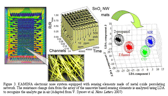
Figure 3. KAMINA electronic nose system equipped with sensing elements made of metal oxide percolating network. The resistance change data from the array of the nanowire based sensing elements is analyzed using LDA to recognize the analyte gas in air (Adapted from V. Sysoev et al. Nano Letters 2007)
|
 properties nano-objects and do it in situ and in real
time.
properties nano-objects and do it in situ and in real
time. These percolating nanowire networks have been implemented as gas sensing elements in real world prototype devices. Namely SnO2 nanowires sensing elements have been combined with commercial KAMINA (Karlsruhe Forschung Zentrum, Germany) electronic micro-nose system Fig.3. Very high gas sensitivity of the metal oxide nanowire sensing elements is complemented by their fast response time. In fact, to our knowledge, these percolating nanowires sensing elements demonstrated one of the best reported sensitivities with pristine SnO2 sensors to carbon monoxide in air. The excellent discrimination power of such gradient gas sensor microarrays apparently stems out of two cumulative contributions — the spatial temperature gradient and (stochastic) nanowire density difference between the individual sensing elements. The latter alone has been found to be sufficient for isothermal gas discrimination between isopropanol, ethanol and CO analytes in air. Overall, gradient microarrays with sensing elements based on metal oxide nanowire mats of different density appear to be a novel and powerful approach for robust, cost effective, sensitive and highly selective nose-like gas analytical devices.
The result of our work have been published in Nano Letters, ACS Nano, Applied Physics Letters and Nanotechnology and widely covered in the media.