Reports: ND555524-ND5: Atomically Thin Size Exclusion Membranes
 printer friendly
SCOPE AND PURPOSE
The fabrication of 2D van der Waals bilayer aluminosilicates with molecule-sized pores has opened the possibility for atomically thin, size-selective membranes with orders of magnitude higher permeances than zeolite membranes.1 As the films have no dangling bonds, delamination from the growth substrate can produce freestanding films which may then be used for separations. The project goal is to study bilayer aluminosilicates as tunable gas separation membranes at the limit of thickness, through the synthesis of bilayers with controlled ring size distributions and subsequent transfer into a membrane test system.
RESEARCH PROGRESS
Growth of tunable silica and aluminosilicates on thin film substrates
The most stable configuration of bilayer SiO2 is a hexagonal six-membered ring structure, which would be sufficient to allow small molecules (e.g. water) to permeate through the structure. Computational work in our group has shown that alternate structures with eight-membered rings that can allow larger molecules to permeate are possible when strain is applied.2 In the first year of the project, we successfully demonstrated a method to produce solid-solution Ni-Pd alloy (111) thin films with continuously-tunable lattice constants and grew a “zero-strain” silica film on the surface with slight (0.93%) compressive strain.4 Scanning tunneling microscopy (STM) of the surface recorded in the last year shows a highly-ordered silicate layer with low defect density, as shown in Figure 1. The alloy films also provide an inexpensive platform for transferring the bilayer silica by etching away the metal, an impractical route for expensive metal single crystals.
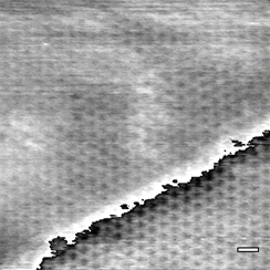
Figure 1: STM of a silica film grown on a “zero-strain” Ni-Pd (111) alloy substrate grown on Cr2O3(0001)/α-Al2O3(0001). Scale bar: 10 Å.
To create larger rings via strain, it is necessary for the silica or aluminosilicate film to interact with the surface strongly enough to maintain registry (commensurate growth). Growth of the “zero-strain” silica film was commensurate crystalline with hexagonal rings, while concurrent experiments in our group demonstrated that high-strain growth on Pd(111) results in incommensurate hexagonal SiO2. To explore the available range of strain which maintains commensurate registry, we synthesized a series of Ni-Pd(111) alloys in range between “zero-strain” and 100% Pd. A phase boundary between commensurate and incommensurate was found to exist between a Ni-Pd lattice constant of 3.790 Å and 3.798 Å, corresponding to 1.12% and 1.34% tensile strain, respectively. Low-energy electron diffraction (LEED) patterns of silica grown on these samples are shown in Figure 2. In contrast to the (2x2) overlayer pattern of commensurate hexagonal silica in Figure 2a, the LEED pattern in Figure 2b exhibits a moiré pattern consistent with incommensurate growth. Work is ongoing to identify the exact transition point and any changes to the ring size distribution which may arise near the boundary.
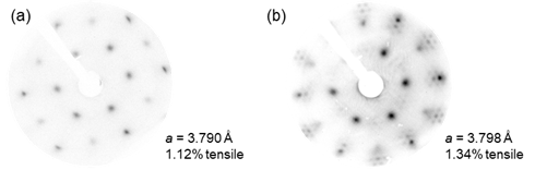
Figure 2: LEED patterns of silica films grown on Ni-Pd (111) alloy substrates with (a) a = 3.790 Å (recorded at 71.0 eV) and (b) a = 3.798 Å (recorded at 69.0 eV).
In parallel with experiments to produce strain-tuned bilayer silica on Ni-Pd (111), we have also grown silica and aluminosilicate films on epitaxial Ru(0001)/α-Al2O3(0001) surfaces. While the surface nearest-neighbor distance of Ru(0001) imparts 2.2% tensile strain on commensurate bilayer silica, it has been shown in previous studies that the resulting bilayer silica film can be produced with highly crystalline character under proper growth conditions.5 In our work, we have managed to produce high-quality films of both silica and aluminosilicates, as demonstrated for an aluminosilicate bilayer in Figure 3. Auger electron spectroscopy (AES) of the sample indicates and expected ratio of Si, O, and Ru on the substrate, while the (2x2) LEED pattern is consistent with a commensurate crystalline aluminosilicate layer with no amorphous character. As experiments proceed to produce freestanding films for the gas permeation test system, growth of bilayers on the Ru(0001) remains a reliable means of producing high-quality films with six-membered rings, with the density of other ring sizes adjustable via the Al concentration.
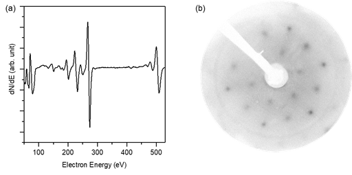
Figure 3: (a) AES and (b) LEED (recorded at 110.0 eV) of an aluminosilicate bilayer grown on Ru(0001)/α-Al2O3(0001).
Delamination and removal of bilayer films
Though purely mechanical transfer of bilayer silica with partial surface coverage has been reported,6 this produces large discontinuities (openings) in the film rendering them incompatible for use as a free-standing membrane. Our work has refined methods for spin-coating PMMA on the surface and removing the bilayer through chemical etching of the inexpensive substrate materials. Recent infrared reflection-absorption spectroscopy (IRRAS) experiments have indicated that Ni silicate phases may form under conditions similar to silica, which would not be as resistant to reaction with the low-pH etchant solutions and may have limited transferability. Further experiments are ongoing to avoid silicate formation and ensure that transferred films are pure silica or aluminosilicate.
SIGNIFICANCE
In the second project year, we have expanded the library of silica and aluminosilicate growth substrates on the path towards tunable ring distributions. Significant progress has been made towards delamination and transfer of the resulting films, which will enable gas permeation testing. Completion of this project will demonstrate the capability of these films to perform size and shape-selective gas separations.
REFERENCES
(1) Kulprathipanja, S. Zeolites in Industrial Separation and Catalysis; John Wiley & Sons, 2010.
(2) Malashevich, A.; Ismail-Beigi, S.; Altman, E. I. J. Phys. Chem. C 2016, 120 (47), 26770–26781.
(3) Huang, P. Y.; Kurasch, S.; Srivastava, A.; Skakalova, V.; Kotakoski, J.; Krasheninnikov, A. V.; Hovden, R.; Mao, Q.; Meyer, J. C.; Smet, J.; Muller, D. A.; Kaiser, U. Nano Lett. 2012, 12 (2), 1081–1086.
(4) Hutchings, G. S.; Jhang, J.-H.; Zhou, C.; Hynek, D.; Schwarz, U. D.; Altman, E. I. ACS Appl. Mater. Interfaces 2017, 9 (12), 11266–11271.
(5) Löffler, D.; Uhlrich, J. J.; Baron, M.; Yang, B.; Yu, X.; Lichtenstein, L.; Heinke, L.; Büchner, C.; Heyde, M.; Shaikhutdinov, S.; Freund, H.-J.; Włodarczyk, R.; Sierka, M.; Sauer, J. Phys. Rev. Lett. 2010, 105 (14), 146104.
(6) Büchner, C.; Wang, Z.-J.; Burson, K. M.; Willinger, M.-G.; Heyde, M.; Schlögl, R.; Freund, H.-J. ACS Nano 2016, 10 (8), 7982–7989.