Reports: ND1057071-ND10: Polymer-Based Processing of Lateral Anionic Superstructures in Complex Oxide Films
 printer friendly
Project Overview: The project goal is to create lateral anionic superstructures and patterns in complex oxide films using a combination of a polymer-based fluorination reactions and lithographic techniques. In particular, it is hypothesized that patterns of alternating (or embedded) SrFe(O,F)3 and SrFeO3-d regions can be stabilized through decomposition of fluoropolymers, which enable fluorination reactions at relatively low temperatures without the use of toxic or hazardous fluorine sources.
Technical Research Progress: Major activities in the first year have focused on developing the microfabrication processes to lithographically pattern and subsequently fluorinate SrFeO2.5 films. Epitaxial SrFeO2.5 films (~25 nm in thickness) are grown by molecular beam epitaxy on single crystalline perovskite substrates. Laser-based photolithography is used to write patterns, which to date have been stripes ranging from 2 to 100 microns in size. After development of the photoresist, a chromium layer is deposited, followed by lift-off of the resist. The chromium layer acts to prevent fluorination of the underlying oxide film, while the areas not cover by chromium are reacted with the fluorine vapor. Fluorination is carried out in a tube furnace at 250°C using polyvinylidene fluoride (PVDF) as the fluoropolymer with argon as the carrier gas. In addition to SrFe(O,F)x / SrFeO2.5 lateral structures, we have also fabricated SrFeO3/SrFeO2.5 lateral superstructures by exposing the patterned film to dilute ozone (5% in O2) in the tube furnace. In both cases, the chromium layers are removed by etching in Chromium Etch 1020ac. Figure 1 summarizes the process for fabricating the anionic superstructures.
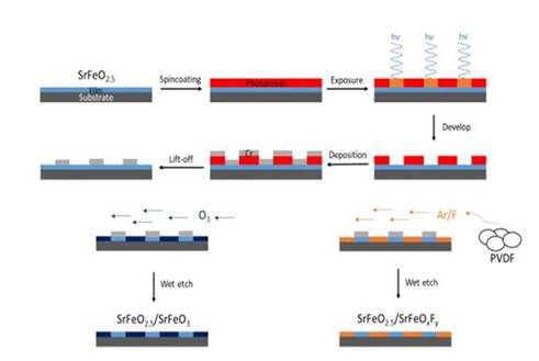
Figure 1. Schematic of the fabrication process used to make SrFe(O,F)x / SrFeO2.5 and SrFeO3/SrFeO2.5 lateral superstructures.
Having established a procedure to fabricate the patterned structures, we are working to ensure that the constituent layers retain their basic physical properties following the various patterning, etching, and reactions steps. Initial work on this front has centered on SrFeO3/SrFeO2.5 superstructures because the physical properties of SrFeO3 and SrFeO2.5 are well established and differ significantly from one another. In structures with 100 micron stripes, we find that the lattice parameters and crystalline quality of the two regions are retained with distinct Bragg peaks for the SrFeO3 and SrFeO2.5 phases present, as shown in Figure 2(a). This result is critical in confirming that formation of the lateral structures does not degrade the material quality. Electrical resistance measurements across the samples are highly anisotropic and exhibit fundamentally different temperature dependences [Figure 2(b)]. With current flowing parallel to the stripes, the resistivity follows that of SrFeO3-d (d ~ 0.05), while when measured perpendicular to the stripes, the resistivity exhibits a basic insulator-like dependence similar to that of SrFeO2.5. This is consistent with behavior expected for the two materials acting as resistors in parallel and resistors in series. The result demonstrates how two fundamentally different sets of conductive behavior can be realized in the same sample through the lateral anionic superstructures.
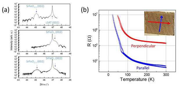
Figure 2. (a) XRD data of reduced SFO (top panel), oxidized SFO (middle panel), and lateral heterostructure (bottom panel). (b) Anisotropic electronic transport measured from a SrFeO2.5/SrFeO3-d laterally superlattice with 100 micron stripes. The resistance measured parallel to the stripes (blue curve) is orders of magnitude lower than the resistance measured perpendicular to the stripes (red curve). The inset displays an optical microscopy image of the sample. The increase in resistivity near 60 K observed in the parallel resistance measurement suggests that the d value in the SrFeO3-d layers is ~0.2, as this charge ordering feature has been previously reported in bulk SrFeO2.81.
As the minimum feature size and abruptness of the interfaces will be limited by lateral diffusion of fluorine to regions covered by the chromium mask during the fluorination process, we have also developed an apparatus to measure resistivity in situ during fluorination (or oxidization). Electrical leads are fed into the tube furnace and connected to external electronics, controlled by a custom Labview program. These measurements will provide direct information on the fluorination kinetics, allowing us to identify the minimum time necessary to fluorinate the structures. By avoiding excess time at elevated temperatures, we hope to minimize lateral diffusion. Example resistance results obtained while oxidizing a SrFeO2.5 film at 130°C are shown in Figure 3.
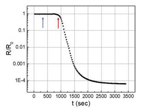
Figure 3. In situ resistance measurement during ozone oxidation of a SrFeO2.5 film. The furnace began heating at the time indicated by the blue arrow and reached 130°C at the time indicated by the red arrow.
There are three major goals for the second year of the project. The first goal is to quantify the extent of lateral diffusion in oxide/oxyfluoride superstructures. To achieve this we have submitted a proposal to the Advanced Light Source to perform photoemission electron microscopy (PEEM) experiments to map out the F concentration with 30 nm spatial resolution. The second goal is to demonstrate how these lateral superstructures enable new functionalities in these materials. We are particularly interested in controlling anisotropic electronic transport and in photonic applications. The third goal is to push the fabrication now to 10s of nanometer feature size by using electron beam lithography instead of optical lithography. We believe this size regime will enable new quantum electronic or optical behaviors.
Impact of Research: The grant has enabled the PI to hire Ben Lefler as a PhD student fully funding through a research assistant position. Ben is a PhD student who started at Drexel in January 2017; Ben received a BS in chemistry from the University of Delaware. An undergraduate student, Evan Dubrunfaut (rising sophomore in materials science and engineering at Drexel), is also working on the project. Evan volunteered two days a week during the summer of 2017 and will continue to do research throughout the Fall quarter. The New Directions Initiative grant has enabled the PI to move his research into a new area of inquiry: lateral superstructures. It is anticipated that this will open new avenues for collaborations in photonics. The PI anticipates submitting at least one grant application to a federal agency focused on optical and photonic properties of these structures in late 2017/early 2018.