Reports: ND552921-ND5: Tailoring Surface Electronic Structure: Probing the Effect on Chemical Activity
 printer friendly
We fabricated 3-dim graphene structures with high surface area using Ni scaffolds that are fabricated using bicontinuous interfacially jammed emulsion gel (bijels) templates. Bijels form via spinoidal decomposition of two immiscible fluids forming bicontinuous domains with colloidal particles jammed at the interface. Electroplating Ni on ethylene glycol coated silica particles then etching the particles forms the Ni scaffold. Heating at 500°C under 4%H2/Ar leads to pyrolysis of ethylene glycol and diffusion of C into Ni. Upon cool down, C segregates to the surface and forms graphene. Fig. 1a is a scanning electron microscopy (SEM) image of a highly porous 3-dim structure after etching the Ni scaffold. Two length scales of pores are observed, with characteristic size of 280 and 2400 nm. Electron dispersive energy spectroscopy shows the structure is primarily composed of C. Raman spectroscopy shows a disordered graphitic signal before etching (blue curve in Fig. 1b). The 2690 cm-1 peak, I2D, is the second-order overtone of in-plane vibration, the 1580 cm-1 peak, IG, is the in-plane vibration of the C-C bond, and the 1350 cm-1 peak, ID, is a disorder peak. By taking the ratio of the I2D /IG peaks, one can determine the number of graphene layers. The red curve of Fig. 1b, after etching the Ni scaffold, is characteristic of few layer graphene (FLG).
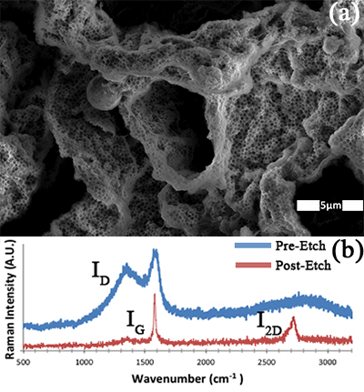
Figure 1: (a) SEM image of FLG structure fabricated with a bijel scaffold. (b) Raman spectra before (blue) and after (red) etching Ni.
We have investigated 2-dim process of graphene formation to elucidate growth mechanisms. An electron-beam evaporator was used to deposit 20 nm of Ni followed by 372nm of Cu leading to a Ni:Cu alloy with composition of 5:95. The photoresists, SU8-2002 and poly-methyl methacrylate (PMMA), were spin coated on substrates. Samples were annealed at 1000 °C under 4% H2/96% Ar. Raman spectra were acquired before and after a 30% FeCl3 etch to remove Ni:Cu to analyze graphene formation on both the Ni:Cu surface and the underlying SiO2 surface as a function of cooling rate. Fig. 2 is Raman spectra of samples annealed with SU8-2002 on Ni:Cu, Fig. 2a (fast cooling) and 2c (slow cooling), and on SiO2, Fig 2b (fast cooling) and 2d (slow cooling). The I2D/IG ratio in Fig. 2b is ~1.26 and is characteristic of trilayer or bilayer graphene. The ratio of Fig. 2d is ~2.29 and is characteristic of SLG. The Raman spectra show that the highest quality graphene film is present underneath the Ni:Cu film with slow cooling. When examining the slow cooling results with PMMA, the Raman spectra are characteristic of FLG on top of the Ni:Cu film and on the SiO2 substrate after etching. The polymer film used as a carbon source thus appears to play a role in the quality of graphene formation to be studied further.

Figure 2: (a) Raman spectra of SU-8 2002 coated sample after a 1000 C anneal on Ni:Cu with fast and (c) with slow cooling and (b) the underlying SiO2 surface with fast cooling and (d) slow cooling.
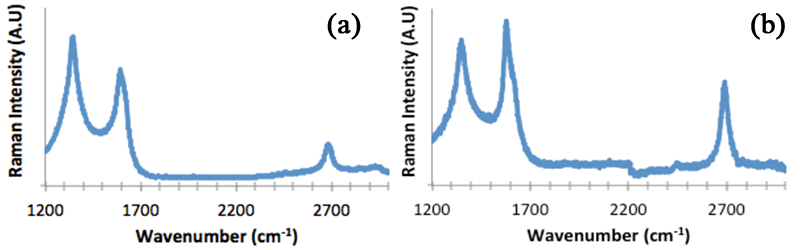
Figure 3: (a) Raman spectra of PMMA coated sample after a 1000 C anneal and (b) underlying SiO2 surface after slow cooling.
Electrochemical deposition of Pt was performed with MLG on 285 nm thick SiO2/p-type Si purchased from Graphene Supermarket. Electrochemical deposition was performed in a 4.8 mM H2Pt Cl6 /0.1 M HCl/0.3 M NaCl solution, purged with Ar gas for 10 minutes. A standard three-electrode setup was used, wherein a potentiostat maintains a potential difference between a working electrode, MLG sample, and a reference electrode, Ag/AgCl, by supplying current to an auxiliary electrode, Pt wire. The working electrode was held at -0.15V with respect to the reference electrode for variable amounts of time at room temperature to perform Pt nanoparticle deposition. After electrochemical deposition, samples were gently rinsed with deionized water, and dried using nitrogen gas. Samples were then imaged using atomic force microscopy to measure nanoparticle width, height, and density. Fig. 4 shows AFM topography images of different samples as a function of deposition time. Pt nanoclusters were observed on MLG samples at deposition times greater than or equal to 15 min. One can observed that nanoparticles grow taller rather than increasing in width with longer deposition time.
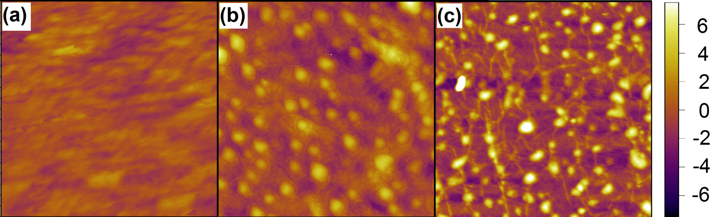
Figure 4: AFM topography images with scale bar on the far right (in nm) of (a) MLG on SiO2, on MLG after (b) 15 minutes and (c) 30 minutes of electrodeposition.
In the remaining grant period we will optimize fabrication of metal hybrid graphene surfaces. We will also characterize surface electronic structure has been identified to be an important factor in chemical activity. We will use scanning Kelvin probe force microscopy (KPFM) and scanning tunneling microscopy (STM)/spectroscopy (STS) to understand the role of processing and morphology on electronic structure and chemical activity. Cyclic voltammetry will be used to measure capacitance and adsorption isotherm measurements in order to determine surface area.