Reports: DNI1050444-DNI10: Investigating Electron-Hole Pair Creation and Lifetimes in Amorphous Hydrogenated Boron Carbide
 printer friendly
Amorphous hydrogenated boron carbide (a-BxC:Hy) is of interest for single-junction wideband photovoltaic energy conversion as it has been shown to produce electron–hole pairs (ehp's) over a large energy range (1.2 to 3.5 eV, or 1000 to 300 nm) with high (>50%) quantum efficiency. The objective of this work is to apply a combined computational and experimental approach to investigate the mechanisms responsible for and lifetimes of ehp generation and recombination in thin-film a-BxC:Hy, grown by plasma-enhanced chemical vapor deposition, in the context of its electronic and physical/chemical structure.
Figure 1. Proposed structural model of amorphous hydrogenated boron carbide (Paquette et al., J. Phys.: Condens. Matter, 2011, 23, 435002)
Understanding charge transport in amorphous hydrogenated boron carbide is uniquely challenging: not only does a-BxC:Hy not display the behavior typical for a crystalline solid, but – being a defect-rich, uniquely bonded, boron-based "molecular solid" – is neither expected to behave quite like traditional inorganic solids such as amorphous silicon nor like the organic electronic materials currently in vogue. Amorphous hydrogenated boron carbide is made up of an extended network of disordered twelve-vertex icosahedra containing hydrogen and varied crosslinking groups (Figure 1), and is expected to exhibit abundant B/C substitutional disorder and defects. Understanding its physical and electronic structure and their relationship to its charge transport properties and mechanisms is nontrivial, but required if it is to be advanced as a possible candidate for photovoltaic energy conversion.
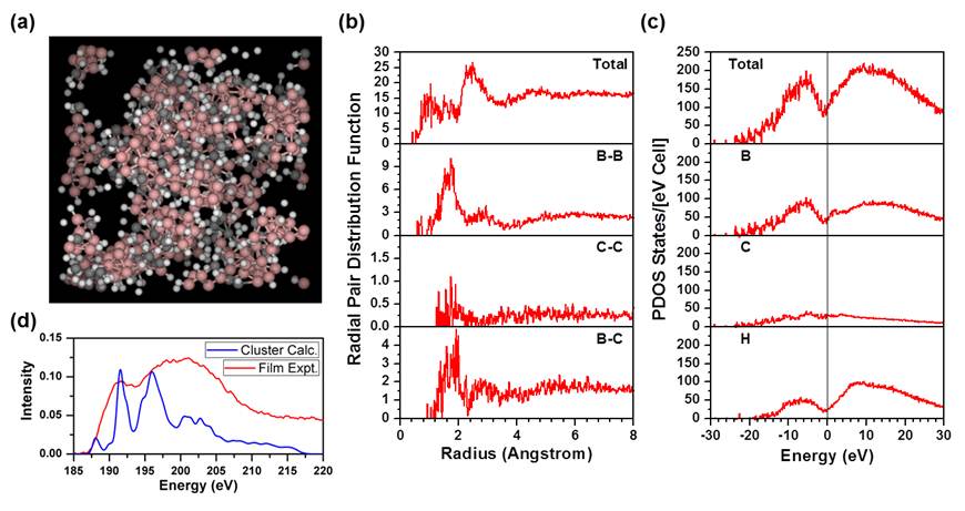
Figure 2. Preliminary results toward the computational modeling of a-BxC:Hy. (a) Periodic amorphous model of a-BxC:Hy produced using a gas-phase molecular dynamics condensation scheme. (b) Radial pair distribution functions computed for the model. (c) Partial density of states for the model computed using the OLCAO method. (c) ELNES boron K-edge spectrum computed from a nanocluster model compared to experimental data acquired for a thin-film sample.
We have made significant progress toward the computational modeling of a-BxC:Hy. To study the electronic structure of a material computationally, structural models are first needed. Modeling amorphous solids is notoriously complex, and the challenge is compounded in the case of boron carbide. Challenges include: the need for large simulation boxes to adequately sample possible local structure variations (rendering many ab initio methods prohibitively expensive), creating a model for a non-directional solid that obeys periodic boundary conditions, and the lack of well-developed interatomic potentials for the unusual 5- and 6-coordinate B and C found in boron-carbide-based materials. Building from work done in the previous year, our collaborator, Prof. Paul Rulis, has continued to refine a hybrid method for modeling a-BxC:Hy. The first step consists of preparing a large simulation box with widely dispersed molecular components in given proportions, chosen based on experimental feedback (more details for which were described in the previous report). The second step involves a gas-phase classical molecular dynamics (MD) condensation scheme in which the components are forced to come together, break or form new bonds, and create a supercell in compliance with periodic boundary conditions. Because the MD results only produce a crude structure, a final ab initio structural relaxation method is applied to obtain the most energetically favorable configuration. Using this method, we have succeeded in generating preliminary models with realistic, yet still imperfect, components and structural parameters (Figures 2(a) and (b)), with which Prof. Rulis has been able to complete preliminary electronic structure calculations via the orthogonalized linear combination of atomic orbitals (OLCAO) method to generate the site-resolved partial density of states (PDOS) (Figure 2(c)) and energy-loss near-edge structure (ELNES) spectra (Figure 2(d)), both of which will be important for evaluating optical/electronic transitions and possible charge transport mechanisms. Additional work to experimentally verify and refine the starting models and predicted electronic structure is in progress.
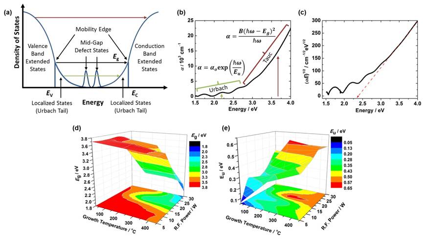
Figure 3. (a) Simplified density of states schematic for a generic amorphous solid. (b) Absorption coefficient as a function of energy obtained from the UV-Vis optical absorption spectrum for an a-BxC:Hy film on glass. (c) Tauc plot derived from the data in (b) to obtain optical band gap. (d) and (e) Optical band gap, Eg, and Urbach energy, Eu, as a function of growth temperature and power for a series of twenty-four a-BxC:Hy films.
Experimentally, we have continued to study the electronic structure for a range of a-BxC:Hy films using various spectroscopies, including optical absorption spectroscopy, spectroscopic ellipsometry, X-ray and ultraviolet photoemission spectroscopies, X-ray absorption and emission spectroscopies, and resonant inelastic X-ray scattering measurements. Using optical absorption spectroscopy, we have studied the optical band gaps, Eg, and Urbach energies, Eu. Unlike in a crystalline solid, in an amorphous solid the band gap is not clearly defined. In addition to the extended/delocalized states which make up the valence and conduction bands, amorphous solids will also exhibit localized states which tail exponentially into the band gap (forming the "Urbach tail"), as well as localized mid-gap defect states (from, e.g., dangling bonds) (Figure 3(a)). A Tauc analysis of the high-energy region of the UV-Vis optical absorption spectrum allows for extraction of the optical band gap (Figures 3(b) and (c)), which defines the edges of the valence and conduction bands; the Urbach energy, a measure of the Urbach tail, can be extracted with an exponential fit to the mid-energy region. We found that Eg and Eu are roughly inversely correlated to each other (Figures 3(d) and (e)), and partially correlated to film density/hydrogen content. Both Eg and Eu play important roles in photoabsorption and photoemission, mobility, and electron-hole pair recombination mechanisms, and precisely understanding their effects in the case of a-BxC:Hy will be critical to optimizing mobility–lifetime products.
Funds from this doctoral new investigator grant have proven invaluable to advancing the PI's research program, a major thrust of which is investigating the electronic structure and charge transport properties of a-BxC:Hy for next-generation device applications. In 2012, Prof. Caruso received the very prestigious University of Missouri President's Award for Early Career Excellence. ACS-PRF funds have supported both an undergraduate and a graduate student, who have received significant experience and training in experimental condensed matter physics, semiconductor device physics, and thin-film materials science.