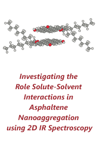
Reports: DNI1051511-DNI10: Silicon Quantum Dot Superlattices for High Efficiency Thermoelectrics
 printer friendly
Increased annual demand for energy has resulted in the burning of more fossil fuels, which have been implicated in global warming. Thermoelectrics are promising materials that can harness waste heat to generate electric power through the Seebeck effect. Significant achievements have been achieved by increasing the thermoelectric figure-of-merit using nanostructured thermoelectric devices. Ideal thermoelectric materials are sometimes referred to as ‘phonon-glass electron-crystals’. Several groups have reported such improvements in ZT by decreasing the thermal conductivity when bulk materials are nanostructured. However, there are almost no studies that show an increase in the power factor. Here we present enhanced thermoelectric power factor in strained Silicon nanomesh thin film superlattices with 36nm pitch and 7-9nm thickness. We report approximately 41.4% improvement on strained silicon thermopower by nanomesh at 300K and overall three times of the power factor in strained Silicon thin film than the unstrained one by nanomesh.
Thermoelectric power factor is defined as S2σ, including thermopwer S and electrical conductivity σ. Together with thermal conductivity κ, it constrains thermoelectric figure-of-merit ZT= S2σT/κ. Compared with metal, semiconductor has larger thermopower due to lower density of charge carriers, which also inevitably sacrifices electrical conductivity due to the interdependent nature of S and σ, largely limiting the energy conversion efficiency. In nanostructured systems, sharp peaks in density of electronic states could lead to higher thermopower and the optimization of dimensions and scales in nanostructures may also yield to an equivalent electrical conductivity yet reduced thermal conductivity to produce higher ZT, provided that the geometrical confinement is larger than the mean free path of charge carriers to free their movement yet smaller than that of phonons to constrain their contribution to thermal conduction. In this report, we demonstrate enhanced power factor in tensile strained Silicon thin film with nanomesh.
Tensile strained Silicon is obtained by depositing a thin layer of Silicon film on a larger crystal lattice so it stretches to match with it (Si1-xGex in this case). Such strained Silicon layer is further transferred to an insulator on Silicon substrate (i.e. SSOI, strained Silicon on insulator) for the convenience of fabrication. Theoretically, phosphorus doped (n-type) tensile strained Silicon could potentially enhance power factor due to a predicted increase on electrical conductivity compared with unstrained Silicon (relaxed Silicon), resulting from the change of electron effective mass due to tensile strain effect. On one hand, in tensile strained Silicon the conduction degenerate bands split into D4 and D2 bands with D2 bands lowered from the original conduction bands D6, easier for Silicon to accept donor electrons. Also, energy redistributes with a band offset of 180meV between D4 and D2 bands, resulting in a decrease in inter-valley band scattering of charge carriers and enabling electron mobility. On the other hand, the light hole band (LH) splits from heavy hole band (HH) in valence bands, causing LH band to have an increased hole effective mass, which leads to a reduced hole mobility and furthermore, a decrease in electrical conductivity. Therefore, n-type doping by phosphorus is preferable for the sake of electrical conductivity. Meanwhile, it is reported that great efforts have been made to prove that holey-like nanostructure with 100nm thickness and 55nm pitch in unstrained Silicon leads to a moderate deteriorated power factor mostly due to a reduced electrical conductivity. The electron depletion at surface states was accounted for such reduction. Thus, the equivalent mechanical strength and superior electrical quality enable strained Silicon with nanomesh to be a viable candidate for competitive thermoelectric power generation purpose, which is expected to exhibit an increased power factor. Independent measurements were conducted for thermopower and electrical conductivity on n-type doped nanomesh strained Silicon thin films, respectively. At the same time, unstrained silicon thin film samples with similar doping level are measured as control samples. In this paper we demonstrate a significant increase of power factor in strained Silicon nanomesh thin film by roughly three times compared with the unstrained one on the thickness scale of 5-9nm, where we employed block copolymer (BCP) lithography to yield nanomesh with 18nm-diameter and 36nm-pitch in long range order.
In this report, we have conducted measurements of thermopower and electrical conductivity on the same sample to integrate data for power factor. Since strained Silicon films have shown excellent potential in electrical conductivity and enhanced thermopower with nanomesh, it is understood that their power factor outweighs unstrained silicon at similar doping impurity level. The best power factor obtained is in strained Silicon thin film without nanomesh, as 4.4×10⁻⁴ W·m/K2 at 300K, followed very closely by the strained Silicon with nanomesh. The power factors of unstained Silicon thin films are reported to be ¼ of the strained one without nanomesh and 1/3 with nanomesh near room temperature. With reason to believe that the thermal conductivity would also be reduced due to nanomesh, it can be concluded that not only the power factor is enhanced by both strain effect and nanomesh, the figure of merit ZT is expected to increase in strained Silicon with nanomesh thin films. Further studies are required to enlighten the prediction.