57th Annual Report on Research 2012 Under Sponsorship of the ACS Petroleum Research Fund
Reports: ND1051514-ND10: Designing Novel Organic/Inorganic Hybrid Architectures for Efficient Energy Conversion
Natalie Stingelin, PhD, Imperial College London
More solar energy impinges on Earth in one hour than all the energy consumed by humans in an entire year. Photovoltaics (PV) technologies that result from the direct conversion of sunlight into electrical energy represent, thus, one of the most obvious alternative sources to fossil fuels. So far, silicon-based devices have not yet provided a fully satisfactory solution, but organic and hybrid structures still lack behind in performance. The objective of this project has been to explore new approaches to organic/inorganic hybrid photovoltaic architectures, gain fundamental understanding of the electronic processes occurring at the organic/inorganic interfaces and the influence of molecular and supra-molecular arrangement on relevant electronic properties. In addition, we also started to integrate complementary competences on materials design, nano-scale characterization, physical chemistry and solid-state physics to address current materials challenges that stifle progress in the hybrid photovoltaics field.
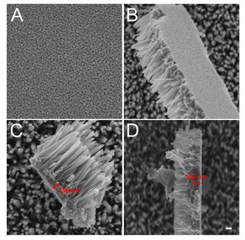
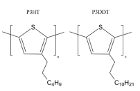
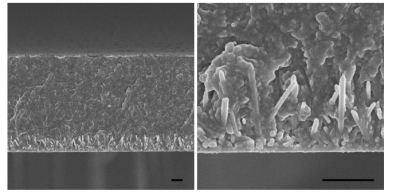
On the science front, our ambition has been to address important materials challenges in the hybrid field and to expand the materials and processing platform. In the first part of the project we thus (i) designed and fabricated well-defined inorganic structures (focus on ZnO), from bi-layers, mesoporous architectures to ordered nanostructures (see Fig. 1), in close collaboration with one of the main project partners (Dr. Martyn McLachlan, Imperial College London). (ii) We controlled the organic/inorganic interface by variation of the polymer deposition onto the inorganic layer, exploring solution-, melt- and solid-state deposition methods. To this end, we used a conjugated polymer that features a melting temperature below 200 °C to avoid degradation when processing the materials from the melt (see Fig. 2). In the second part of the project we now will focus on manipulating the microstructure of the organic macromolecular component (e.g. by crystallization at elevated temperatures, use of nucleation agents.)
Fig. 1. Scanning electron micrographs of a ZnO seed layer in top view (A) and the seed layer as attached to ZnO nanorodes (B-C). The thickness of the seed layers is in the ragne of 150 nm and 160 nm (Scale bar: 100 nm)
In addition to our research activities, we used the support supplied by the ACS Petroleum Research Fund to advance the scientific education of a number of postgraduate students (MSc, MRes, PhDs) as well as postdoctoral researchers. We integrated these early career scientists into the project and provided them with the support to spend some time for field work experiments at partner institutions. For instance, at the University of California Santa Barbara, USA, they were trained in inter-diffusion experiments of organic:organic and organic:inorganic
A Fig. 2. A. Chemical structures of the melt processable polymeric
semiconductors we have focused on in the first part of the project. P3DDT was
selected because of its melting temperature of 180 °C. B. Scanning electron
micrographs of ZnO nanorods fully filled with P3HT by melting the polymer into
substrate. In strong contrast, solution processing did lead only to partially
filling. In the second part of the project, pathways will be explored to reduce
the thickness of the remaing bulk polymer film on the ZnO rods. junctions, using dynamic secondary ion mass spectrometry (D-SIMS).Other students conducted also field work activities at the University of
Nova Gorica (Slovenia) to learn on lateral time-of-flight photoconductivity
measurements; other field work activities encompassed them to learn about
thin-film fabrication and characterisation for use in thin-film transistor at
the Holst Centre in Eindhoven (NL); density measurement of the various organic
structures (at the Swiss Federal Institute of Technology in Zürich,
Switzerland) to relate e.g. degree of crystallinity with device performance.
Students also attended beam times at the Synchrotron at Grenoble to identify
the different polymorphs of the inorganic structures produced. Students
involved in the project and that participated in those field trips were
Recipient of the 2012 Imperial College's Physics Postgraduate Research
Symposium Prize for "best overall poster for clarity of communication and
enthusiasm" and Recipient of the "highly commended prize" at Imperial
College London's Graduate School symposium on 19th June 2012.

