Reports: ND1048813-ND10: Renewable Energy from a Neglected Photovoltaic Material: Boron Arsenide
 printer friendly
Compound main group semiconductors possess several electronic properties that are superior to those of silicon, thus making them suitable for a variety of novel applications.[1] Boron arsenide (BAs) is of particular interest to us because it is isoelectronic with silicon and has good prospects for photovoltaic and photoelectrochemical applications. Interestingly however, it has long been neglected in the study of compound main group semiconductors. Boron arsenide is the most covalent of the family of III-V compounds and theoretical investigations have revealed that boron may even act as the anion in this nearly perfectly covalent compound.[2]
Granular boron (0.42 to 4.75 mm) was treated with two molar equivalents of arsenic in sealed, evacuated quartz tubes that were heated to 800 °C. SEM images of the product, which are displayed in Figure 1, revealed that an interesting surface reaction had taken place, resulting in the deposition of a thin layer of BAs on top of the boron substrate. The presence of polycrystalline BAs and elemental boron was established on the basis of XRD data taken from a single piece of the material. High-resolution XPS spectra revealed a mole ratio of boron and arsenic close to unity, thus indicating broad BAs thin layer coverage on the boron substrate.
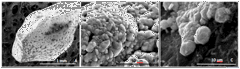
Figure 1. SEM images reveal the surface and core structure of the boron arsenide containing material prepared from granular boron. (A) A single piece of BAs. (B) Area of continuous BAs surface coverage. (C) Area featuring a gap in surface coverage. The light material is BAs and the dark material is the boron substrate.
This BAs electrode displayed p-type behavior and was photoactive under both visible (wavelength > 420 nm) and UV-visible light irradiation in Figure 2. The the linear sweep voltammograms (LSVs) spanned a potential range of 0.0 to - 0.5 V vs. Ag/AgCl at a scan rate of 20 mV/s. The voltammetric measurements, which were carried out in a 0.1 M Na2SO4 aqueous solution containing 0.01 M methyl viologen (MV2+), showed a cathodic photocurrent attributable to the reduction of MV2+. The Figure 2(A). Figures 2(B) and (C) display the corresponding current-potential curves for a BAs crystal using chopped visible and UV-visible light irradiation, respectively.
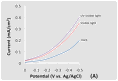
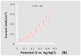
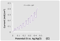
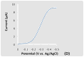
Figure 2. LSVs in a 0.1 M Na2SO4 aqueous solution containing 0.01 M methyl viologen. The potential was swept from 0.0 V to -0.5 V vs. Ag/AgCl at a scan rate of 20 mV/s. The incident light intensity at the electrode surface was 100 mW/cm2. (A) Current flow for the BAs material in the dark, under visible and UV-visible light irradiation. (B) Current flow for the BAs material under chopped visible light irradiation. (C) Current flow for the BAs material under chopped UV-visible light irradiation. (D) A LSV of an arsenic doped boron electrode in the dark.
The origin of the dark current from the BAs crystal is still not clear and requires further investigation, although an As-doped boron electrode exhibited a dark current, as shown in Figure 2(D). However, no photocurrent was detected with this electrode under the same conditions as those described in Figures 2(A), (B) and (C). As shown in Figure 3, the net photocurrent, after subtraction of the dark current, is approximately 0.1 mA/cm2 under full Xe lamp irradiation at an applied potential of -0.25 V vs. Ag/AgCl.
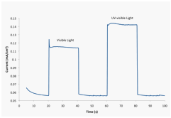
Figure 3. Current at an applied potential of -0.25 V vs. Ag/AgCl in the dark (0-20 s, 40-60 s, and 80-100 s), under visible (wavelength > 420 nm) light irradiation (20-40 s) and under UV-visible (Xe lamp) light irradiation (60-80 s).
Mott-Schottky plots in Figure 4, were obtained for this BAs electrode in the potential range of 200 Hz to 1 KHz. The estimated flat-band potential appears to be approximately 0.5 V vs. Ag/AgCl. The flat-band potential was also estimated by measuring the onset photopotential. A LSV spanning the potential range of 0.45 to -0.4 V vs. Ag/AgCl, as shown in Figure 5, revealed that the onset photopotential of the p-type BAs electrode is ~ 0.35 V vs. Ag/AgCl.
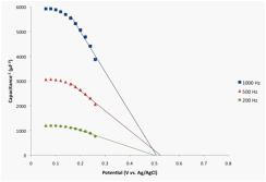
Figure 4. Mott-Schottky plots of the BAs electrode in the dark. The AC modulation amplitude was 10 mV peak-to-peak.
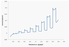
Figure 5. Overall current for the BAs electrode under chopped UV-visible light irradiation.
The photocurrent for the BAs crystal was measured as a function of wavelength over the range 350 to 850 nm using a Xe lamp and a monochromator. The incident photon-to-electron conversion efficiencies (IPCE) were calculated on the basis of the following equation:
IPCE (%) = 1240 × (iph / λ� Pin) × 100
In the above equation, iph represents the photocurrent (in mA) measured at - 0.25 V vs. Ag/AgCl, λ is the wavelength (in nm), and Pin represents the incident light intensity (in mW) at the surface of the semiconductor electrode. The IPCE plot is displayed in Figure 6.
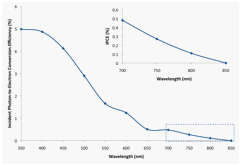
Figure 6. IPCE from the BAs crystal calculated from the net photocurrent at -0.25 V vs. Ag/AgCl.
The calculated IPCE values reached ~ 5% at 400 nm for the selected BAs crystal. The IPCE values decreased with increasing wavelength and reached zero at approximately 850 nm. As a consequence, the estimated indirect band gap[3],[4] is 1.46 ± 0.02 eV, which agrees well with the literature values[5],[6] and values derived from theoretical calculations.[7],[8],[9]
[1] Malik, M. A.; Afzaal, M.; O'Brien, P. Chem. Rev. 2010, 110, 4417.
[2] Boudjemline, A.; Islam, M. M.; Louail, L.; Diawara, B. Physica B 2011, 406, 4272 and references therein.
[3] Butler, M. A. J. Appl. Phys. 1977, 48, 1914.
[4] Johnson, E. J. In Semiconductors and Semimetals; Willardson, R. K.; Beer, A. C., Eds.; Academic Press: New York, 1967; Vol. 3, Chapter 6.
[5] Ku, S. M. J. Electrochem. Soc. 1966, 113, 813.
[6] Chu, T. L.; Hyslop, A. E. J. Electrochem. Soc. 1974, 121, 412.
[7] Merabet, M.; Rached, D.; Khenata, R.; Benalia, S.; Abidri, B.; Bettahar, N.; Bin Omran, S. Physica B 2011,406, 3247 and references therein.
[8] Cohen, M. L. Phys. Rev. B. 1991, 43, 9126.
[9] Hart, G. L. W.; Zunger, A. Phys. Rev. B; Condens. Matter Mater. Phys. 2000, 62, 13522.