Reports: DNI1051099-DNI10: Thin Film Absorber Solar Cells Using Earth Abundant Materials
 printer friendly
Hematite constitutes one of the most promising semiconductor materials for the conversion of sunlight into chemical fuels by water splitting. This promise emanates from its unique combination of desirable properties: a 2.2 eV bandgap that allows the absorption of a significant fraction of sun light, an abundance of iron in the Earth's crust, an extremely low materials cost, and electrochemical stability. The effective use of Hematite as a photoelectrode has generally been prevented, however, due to the short minority carrier mobility and lifetime which results in a very short charge collection length. The goal of our ACS-PRF supported research is to investigate the possibility of utilizing thin films of hematite, prepared via atomic layer deposition (ALD), as a way of overcoming the short charge collection length. This work is driven by systematic investigations of the fundamental structure-function relationships of hematite thin films in water splitting applications. In addition, use of ALD allows us to deposit hematite thin films on high aspect ratio transparent conductive oxide (TCO) substrates in identical fashion as the model thin films, which result in increased light absorption while maintaining the advantages and properties of the model thin film electrodes
We employed Impedance Spectroscopy (IS) to investigate the photoelectrochemical behavior of hematite electrodes under water splitting conditions. The Impedance spectra are characterized by the existence of a prominent surface state, which follows classical behavior in terms of the capacitive features and the dependence on voltage and illumination intensity. The strong correlation between the trap and the photocurrent onset indicated that the hole-transfer step leading to water oxidation takes place predominantly from surface trapped holes, and not directly from valence band holes. We then compared the photoelectrochemical behavior of hematite electrodes in contact with H2O and [Fe(CN)6]3-/4- electrolytes using a combination of IS, photocurrent transient and cyclic voltammetry measurements to determine the cause of the large overpotential required for water splitting. We were able to deduce the physical meaning of photogenerated holes being trapped at the surface as the first step in the water oxidation process, specifically the reversible oxidation of surface hydroxide species. It is only after a buildup of these oxidized intermediates that water oxidation proceeds. Further, we clearly identified surface state recombination as the process which primarily limits the efficiency of water oxidation. Work is ongoing in our lab to further clarify and overcome these limitations.
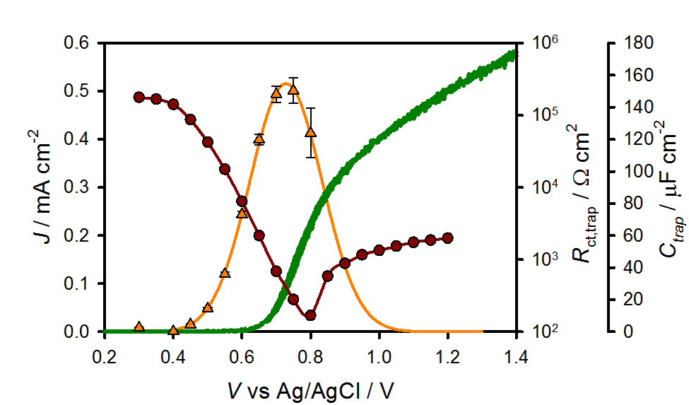
Figure 1. J(V) curve (green solid line), Ctrap (orange triangles) and Rct,trap (red circles) values obtained for a 60 nm hematite electrode under 1 sun illumination and pH 6.9.
Initial efforts to increase the light absorption of these thin film hematite electrodes through nanostructuring included fabricating high surface area transparent indium tin oxide inverse-opals (ITO-IO) as the substrate which can subsequently be coated with hematite via ALD. Briefly, the synthesis of indium doped tin (IV) oxide inverse opal films (ITO-IO) was conducted by drop-casting polystyrene nanospheres (350 ± 14 nm) onto ITO glass. The nanosphere template was infiltrated with and ITO solution by drop-casting and after annealing, the ITO-IO structures remained on the ITO glass (Figure 1). Thin films of hematite were then deposited onto the IO structures using ALD. The resulting hematite coated ITO-IO where characterized using SEM, UV-Vis spectroscopy, and photoelectrochemical measurements. So far, the α-Fe2O3-coated ITO-IO electrodes were found to absorb ~50% more light over all measured wavelengths compared to the absorption planar hematite electrodes prepared with the same thickness. The incident photon to current efficiency data indicated improved external quantum efficiencies for the ITO-IO structures compared to the planar ITO films, however the internal quantum yield was reduced. In other words, while the photocurrent did increase upon scaling up the light absorption with the ITO-IO substrates, the improvement has not been as significant as we expected. We are currently investigating the cause of the decreased internal quantum yields.
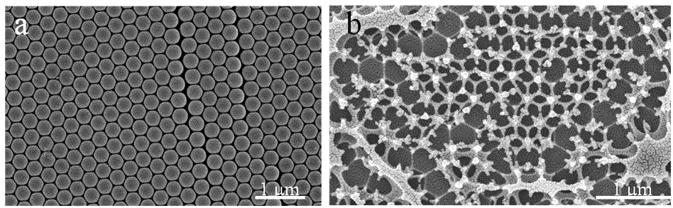
Figure 2. SEM images of a) self-assembled polystyrene nanospheres on ITO and b) ITO-IO structures on ITO glass after annealing.
This ACS-PRF grant has been effectively used to attract and support the work of two graduate students. One of the graduate students will be defending his PhD in spring 2013, thanks in part to support from this grant. The results from this project have been presented several national and international conferences and resulted in multiple publications in top journals (J. Am. Chem. Soc. 2012, 134, 4294-4302, Dalton Trans., 2012, 41, 7830-7834, Energy Environ. Sci., 2012, 5, 7626-7636). The results presented in this progress report also formed the basis for funded NSF CAREER Award proposal, which will help support additional students and allow further directions related to this work to be pursued in the future. Thus, the award of this grant, which was my first award, has been instrumental in advancing my career.