AmericanChemicalSociety.com
Reports: DNI10 49790-DNI10: Harnessing Surface Plasmon Subwavelength Optics in Metallic Nanostructures for Enhanced Efficiency in Thin-Film Solar Cells
With the support of the ACS-PRF DNI grant, we have made significant progress in the development of nanostructured plasmonic electrodes for photovoltaics. "Plasmonics" is the rapidly emerging field of using metallic nanostructures, which exhibit "plasmon" oscillations of the free electrons, for the sub-wavelength control and confinement of optical energy. The goal of this DNI project is to use such nanostructured metal films as semi-transparent electrodes to improve the optical absorption and power conversion efficiency of thin-film solar cells. To address the challenges of fabricating large-area patterns with nanometer-scale resolution, we employed nanosphere lithography (NSL) technique. Self-assembly of colloidal nanospheres into a hexagonal array was followed by a reactive ion etch step to shrink the nanospheres before metal deposition, which allowed the formation of periodic nanohole arrays after removal of the nanospheres (Fig. 1). By controlling the polystyrene nanosphere size (400~600 nm), etching time, metal deposition thickness and angle, it is possible to tune the nanohole spacing, shape, size and their subsequent plasmonic properties. In contrast to other techniques, NSL offers key advantages for low-cost processing because it does not require an expensive photolithography mask or imprint mold, eliminates high capital costs for exposure tools, and provides high-throughput fabrication over a large substrate area. With this technique, we can fabricate patterned periodic nanohole arrays on a 1~2 cm2 metal film on glass substrates. We are developing wafer-scale fabrication technique to pattern these nanohole electrodes with higher throughput and further improved plasmonic properties.
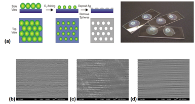
Fig. 1. Fabrication of self-assembled plasmonic nanohole arrays. NSL scheme and samples made on glass slides (a) to make a self-assembled periodic nanoholes. (b) Packed nanospheres (c) after RIE, and (d) after bead removal (200 nm diameter, 600nm pitch, 50 nm thick silver film).
Subsequently, these NSL-patterned metal electrodes were integrated with organic photovoltaic cells (OPV). With traditional diffraction-limited optics, confinement and control of the optical field within the photoactive layers is difficult, resulting in the need for the subwavelength optics of surface plasmons (SPs). Due to their evanescent nature, SPs are confined to a metal interface, decay exponentially away from it, and cannot directly re-radiate into free space. Because surface plasmons are able to confine a significant amount of optical energy within a volume well below the diffraction limit, they can increase light-matter interactions in thin-film photovoltaic cells and lead to enhanced optical absorption and power conversion efficiency. However, SPs carry a certain amount of extra momentum due to their coupling with electrons, therefore requiring the use of specialized coupling geometry, such as an array of nanoholes, to excite SP modes with incident light.
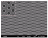
Figure 2: Ag electrode patterned using NSL (periodicity: 600 nm, hole size: 300 nm).
The PI and collaborator (Prof. Russ Holmes in Chemical Engineering) have made progress on the demonstration of OPVs integrated with plasmonic nanohole arrays using NSL (Fig. 2). This work builds our previous, more exploratory work on small device area plasmonic OPVs constructed on one-dimensional arrays of nanoslits. In the present work supported by the ACS DNI grant, the PI sought to explore the viability of using engineered plasmonic electrodes and demonstrate a performance that matches OPVs constructed on a conventional indium tin oxide (ITO) electrode. Periodic nanohole electrodes with their optical properties tuned for OPV absorption bands were patterned over a 1 cm2 area, resulting in OPV device performance equal to that of a conventional ITO-based architecture.
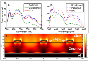
Figure 3:(a) Simulated and (b) Experimental device performance of CuPc:C60 OPVs deposited on an Ag electrode patterned with a hexagonal array of 300nm holes with a 400nm periodicity. The structure of the devices is 14 nm Ag/20 nm CuPc/40 nm C60/10 nm BCP/50 nm Al. (c) Cross-section of the OPV device described above showing the field intensity within the device when illuminated at 622nm showing a plasmonic resonance.
Subwavelength, nanostructured Ag contacts are shown in Fig. 2. Organic layers consisting of a 20-nm-thick layer of CuPc, a 40-nm-thick layer of C60, and a 10-nm-thick film of BCP were deposited on the patterned Ag anode (12 nm thickness). The structure was capped with a 50-nm-thick Al cathode defining a device diameter of 1 mm. Device performances for patterned Ag, unpatterned Ag, and an ITO-based OPV under simulated AM1.5G solar illumination were measured. Overall, no change in device fill factor (FF) is observed with patterning, indicating that removing silver during patterning does not adversely affect the collection of dissociated charge carriers, and that the enhancement effects seen are purely optical. This is encouraging as initial concerns of using patterned metallic electrode were increases in resistance and hence a reduction in FF. Both the responsivity and power conversion efficiency of the device increase with patterning, and the patterned device shows performance that is comparable to a device using a standard ITO anode.
Along with the experimental trials we have used 3D finite-difference-time-domain (FDTD) simulations of the electromagnetic properties of the system to both confirm our findings and more easily optimize our system. Figure 3 shows a comparison between the experimental and simulated spectral response. The spectral response of the simulated structure is modeled by calculating the amount of power absorbed within one exciton-diffusion length of the organic donor-acceptor interface since in an OPV device the majority of the photocurrent is generated by the photons absorbed within this region. Comparison of the spectral data show similar trends in the experimental and simulated data indicating improved performance with pattered electrodes over similar, but unpatterned, Ag electrodes and comparable performance to an ITO electrode. Figure 3C shows the total field intensity inside the device at a wavelength of 622 nm, one of the absorption peaks of the organic materials. The nanohole periodicity was tuned so that a plasmonic resonance would be generated at this wavelength to increase the field intensity which in-turn would increase the absorption in the organic materials.
[1] S.H. Lee et al., Langmuir 25, 13685 (2009).
