AmericanChemicalSociety.com
Reports: G10 48227-G10: A Systematic Study on Vapor-liquid-solid (VLS) Growth Process of Metal Oxide Nanodendrites
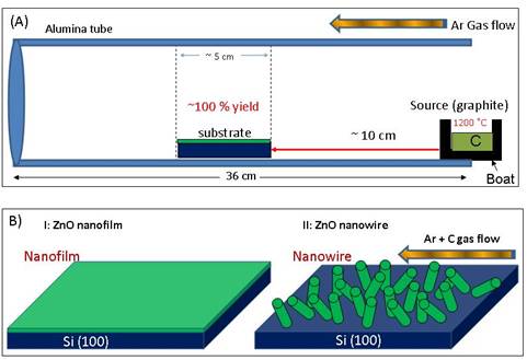
In the last report, the graphite was found to demonstrate a unique ‘catalyst' effect on in-situ conversion of ZnO nanofilm into nanowires and into nanodendrites. To investigate the graphite effect, a comparative experimental and theoretical study has been carried out. To start with, ~3 gram graphite powder loaded was used as the source material and kept in the tube furnace center, as shown in the Fig. 1a. Silicon substrate sputtered with 50 nm ZnO nanofilm was placed ~10 cm away from the source. During the experiment, the furnace was heated to 1200 °C with a 25 °C/min ramping rate and kept for 2 hours. The pressure was controlled at ~100 mbar when temperature reached 1000 °C and carrier gas Ar was initiated at 20 sccm. During the cooling period, Ar gas was stopped when temperature reached at 1000 °C. Fig. 1b shows the schematic of final result where silicon substrate sputtered with ZnO nanofilm (50 nm) converted into uniformly distributed ZnO nanowires with a ~100 % yield at a temperature range of ~800-900 °C. A JEOL JSM 6335F field emission SEM and an FEI Tecnai 12 STEM were used to characterize the morphology and structure of the converted nanowires. The composition was determined by EDX spectrometers attached to the SEM and TEM.
Fig. 1 (a) A schematic in-situ
carbothermal set-up of ZnO nanowires. (b) A Schematic diagram of ZnO nanofilm conversion
into ZnO nanowires in the presence of graphite source and carrier gas
flow.
Fig.
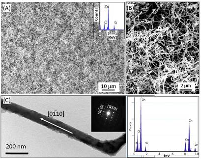
2a is a top-view SEM image of large scale as-converted zig-zag ZnO nanowire and
the inset displays the EDX spectrum revealing the presence of Zn, O and Si.
Silicon peak appears due to the Si substrate. Fig. 2b shows the converted ZnO
nanowires ~100 nm wide and microns long. A typical TEM image of zig-zag ZnO
nanowires and the corresponding selective area electron diffraction (SAED)
pattern in Fig. 2c reveals the single crystalline wurtzite structured nanowire
grown along [01-10] direction. Fig. 2d is an EDX spectrum of a single nanowire
confirming the composition of ZnO nanowire, while the copper peak due to TEM
grid. Here, sputtered ZnO nanofilm has a (0001) orientation as proved by the
x-ray diffraction pattern shown in Figure 3a, which is energetically more
favorable, compared to (11-20) and (01-10). The zig-zag nature of the grown ZnO
nanowires with growth direction of [01-10] is consistent with the early report
suggesting that zig-zag structure of nanowires results from the periodic change
in equivalent growth directions of <01-10>, i.e., from [1-100]à[10-10]à[01-10]à[10-10].8
Fig. 2 (a) Low magnification SEM image
of zig-zag ZnO nanowire. Inset picture shows the EDX spectrum of ZnO nanowires.
(b) high magnification SEM image. (c) TEM image of ZnO nanowire and inset shows
the SAED pattern of the nanowire with growth direction along (01-10). (d) EDX
spectrum of single nanowire in TEM.
In order to investigate the
conversion process of [0001] oriented ZnO nanofilm into [01-10] nanowires, an
array of comparative experiments has been designed and conducted, as listed in
table I.
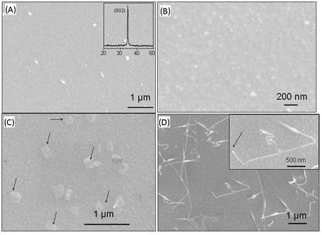
Table 1.
Temperature Duration (minutes) Argon (20 sccm) Carbon (~3g) Result 1200 °C 60 absent absent Nanoislands formation (Fig. 3a) 60 present present Bigger nanoisland formation due to coarsening (Fig. 3c) 90 present present Nanowires grown from nanoisland, ~30-40% yield (Fig. 3d) 120 Present Present ~100 % yield ZnO nanowire (Fig. 2a-b) The involvement of graphite and
Ar flow simultaneously has been suggested to be necessary through the
experiments observations and rational comparison. With a 50 nm ZnO coated
silicon substrate subjected to the annealing at ~800-900 oC for 1
hour in absence of graphite and carrier gas, 20-50 nm ZnO nanoislands formed
quite uniformly (Fig. 3). The inset x-ray diffraction pattern in Fig. 3a shows
that the nanoisland-based ZnO film kept its textured (001) orientation. The high
temperature process clearly transforms as-sputtered ZnO nanofilms from smooth
flat surfaces to rough surfaces with coarsened grain.9 These
nanoislands still has preferential alignment along (001) direction after
annealing. Upon annealing for 1 hour at 800-900 oC, with Ar carrier
gas and graphite source (Fig. 3c), the ZnO nanoisland size further increased
and some nanoislands were bigger compared to others due to coarsening effect.
This coarsening phenomenon is due to a natural self-organization of the surface
adatoms driven by the reduction of surface area, therefore surface energy. The
equilibrium state could not be attained here, as the nanoisalnd ripening
process is opposed by diffusion or interface mass-transfer barriers. With
graphite source and Ar carrier gas, another hour and half long annealing
process clearly bring up the nucleation and growth of nanowires, as evidenced
in Fig. 3d. These nanowires are 2-10 mm in
length and less than 100 nm in diameter. Inset picture clearly shows that
nanowire has grown from the nanoisland as indicated by an arrowhead. This
result suggests that as the temperature increases, nanofilm breaks down into
the nanoislands12 (Fig. 3c), with increasing temperature, induced
stress on the nanofilm leads to the formation of nanorods or nanowires to
reduce the surface energy and the pass-by gas flow (carbon + Ar) during
synthesis could provide the transient reduction and in-situ recombination of
comprised atoms in the deposited compound (Zn-O in our case), therefore could
favor nanowires formation11.
Fig. 3 (a) A typical SEM image of ZnO-coated
silicon after 1-hour annealing in absence of graphite source and Ar carrier
gas. Inset shows the XRD pattern retaining (001) orientation before and after
annealing of 50 nm ZnO sputtered silicon substrate. (b) high magnification SEM
image revealing nanoisland formation. (c) SEM image of sputtered ZnO nanofilm
for 1 hour in presence of graphite source and Ar carrier gas. (d) ZnO nanowires
grown from the nanoisland at 1 hour 30 minute in presence of Ar and graphite.
Inset picture shows that nanowire growing from nanoisland.