AmericanChemicalSociety.com
Reports: DNI10 48796-DNI10: Direct Growth of Type II Core/Shell Nanowire Array on Transparent Conducting Oxide (TCO) Substrate for Potential Solar Cell Application
The use of quasi-one-dimensional, vertically aligned nanostructures to construct three-dimensional architectures as building blocks for photovoltaic (PV) devices, boosting charge transport and collection and/or enhancing light absorption, has demonstrated advantages over conventional planar devices. Beside the conventional p-n junctions, an alternative strategy relying on type II band alignment has been proposed to achieve the lateral charge separation in the core/shell nanowire solar cells. ZnO and ZnS, a representative II-VI semiconductors combination to from type II heterojunction, has been theoretically predicted to possess a band gap of 2.07 eV in the form of nanoscaled core-shell geometry. In additional, ZnO and ZnS are composed of abundance elements in the earth crust, which may open the avenue to obtain low-cost and nontoxic PV devices. During this funding period, we have focused on ZnO/ZnS core shell nanowire array growth as well as PV prototype fabrication. The details are as follows.
ZnO/ZnS nanowire array was first synthesized by combining two-step synthetic procedures combining chemical vapor deposition (CVD) for ZnO nanowire array growth and pulsed laser deposition (PLD) for the shell coating. Fig. 1(a) shows a typical low-magnification SEM image of an as-synthesized large-area ZnO nanowire array, revealing perpendicular growth of ZnO nanowires on the ITO glass. The ZnO nanowire array, as shown in Fig. 1(b), has an average length of ~7 μm and diameters in the range of 50~120 nm. SEM image of the nanowire array after the pulsed-laser deposition of ZnS is presented in Fig. 1(c). Compared with the bare ZnO nanowire, a noticeable increase in the diameter and rough surface for the ZnO/ZnS nanowires was also observed. The sharp interface between the core and shell clearly suggests that the ZnO nanowire is fully sheathed along the entire length. The ZnS layer is ∼12 nm thick and has a rough surface (Fig.2(a)). Further detailed investigations reveals that the marked inter-planar d spacings of 0.31 and 0.52 nm correspond, respectively, to the (-11-1) lattice plane of ZB ZnS with the [011] zone axis and the (0001) lattice plane of WZ ZnO with the [2-1-10] zone axis. Therefore, the core and shell are determined as epitaxial growth with the growth relationship of [0001]ZnO//[-11-1]ZnS and [01-10]ZnO//[211]ZnS (Fig.2(c) and (d)). Without applying external bias, the photocurrent generated in the PV device (Fig.3(c)) based on ZnO/ZnS core-shell nanowire array increased/decreased faster and represented 30 times stronger than that observed in the device composed of a bare ZnO nanowire array with the same active area, as the incident light (AM 1.5 G) was turned on/off (Fig. 3 (a)). The enhanced photocurrent and faster response observed in ZnO/ZnS, together with the quenching of the UV emission, could indicate the realization of the key feature of the type II heterostructure -- the charge separation, although other possibilities (such as the ZnS/Au contact is different from ZnO/Au) cannot be completely excluded. However, because of the large thickness of the nanowire layer, the light absorption occurs mostly in the bulk part of the ZnO nanowire core, the core-shell interface has to serve the function of separating the electrons and holes. Fig.3(b) shows the current-voltage (I-V) curve of the device under an illumination of 1,000 W/m2. The Voc is0.09 V, with a FF of 0.28. The energy efficiency could not be given because of the uncertainty of the actual device area. Although the device performance is far from satisfactory, this prototype device demonstrated the feasibility of fabricating a core-shell nanowire solar cell based on the type II heterostructure and a whole array of such devices.
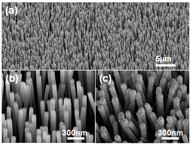
FIG.1 (a) SEM image of a well-aligned ZnO NW grown on ITO substrate. (b) and (c) Magnified SEM images of bare ZnO and ZnO/ZnS core-shell NW arrays. respectively.
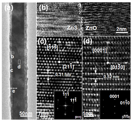
FIG.2 HRTEM Structural characterization of ZnO/ZnS core-shell nanowire array.
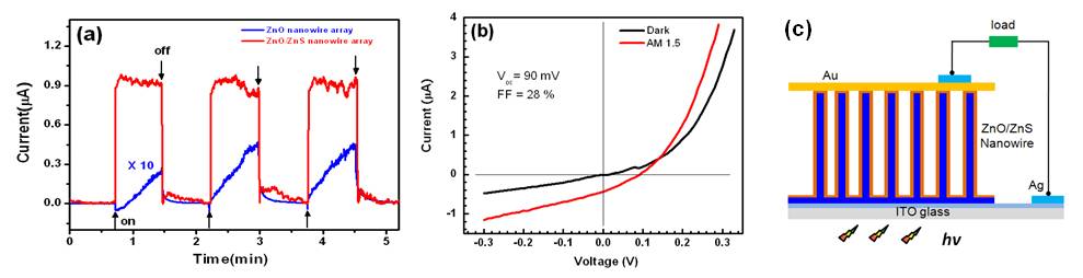
FIG.3 (a) Time-dependent photocurrent of bare ZnO and ZnO/ZnS core-shell NW arrays without external bias. (b) PV effect for the solar cell in the dark and under simulated solar illumination. (c) The prototype of the PV devices based on ZnO/ZnS NW arrays.
In summary, a large area well aligned air-stable ZnO/ZnS core-shell nanowire array was fabricated directly on ITO substrate by combining CVD and PLD techniques. Morphologies and Structure studies showed that the ZnO nanowire array was uniformly and perpendicularly grown on the ITO substrate and the shell with a thickness of 5~10 nm were epitaxially grown on the ZnO nanowires core. The charge separation in the ZnO/ZnS nanowire array was investigated by the PL and photoresponse based on the type II heterojunction-based perpendicular device. To improve the solar conversion efficiency of the type II PV devices, further investigation will address the issues including optimizing the parameters of synthesis of materials and fabrication of devices, designing novel ZnO nanostructure with controllable geometries, and searching for II-VI semiconductor combinations with less lattice mismatch.
