
46777-G10
Fundamental Investigations of the Microstructure of Semicrystalline Polymers for Alternative Energy Generation
There has been great interest recently in structure-property relationships of conjugated polymers. Indeed, this class of materials has found applications in the fabrication of low-cost electronic devices such as thin-film transistors, light-emitting diodes or photovoltaic cells. The two latter applications are of particular relevance in tackling the energy challenge. Light-emitting diodes can potentially replaceme incandescent or fluorescent light bulbs leading to energy conservation. Photovoltaic cells on the other hand can be used to produce cheap energy from sunlight.
Currently, the most promising organic solar cells have a structure known as bulk heterojunction (BHJ) and are an inorganic/organic hybrid device. In these devices the polymer and its inorganic counterpart are intermixed at the nanometer scale. Polythiophenes are a promising family of conjugated polymers for BHJ solar cells. These materials form semicrystalline microstructures when cast into thin films. The microstructure of polythiophenes plays an important role in the power conversion efficiency of photovoltaic cells. Characterizing polymers in BHJ cells however is challenging because of the nanoscale structure and because of the inherent differences between the organic and inorganic components.
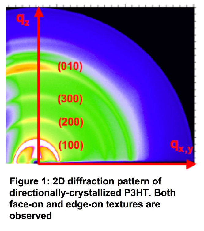
As a first step towards tackling this problem, we performed x-ray diffraction of thin films of polythiophenes on SiO2 where the polythiophene was biaxially textured using a directional crystallization technique. We used poly(3-hexylthiophene) (P3HT) as a model polythiophene because it is the most studied semicrystalline semiconductor. This system was chosen because the texture would make transmission electron microscopy (TEM) of the organic/inorganic interface somewhat easier. The X-ray diffraction pattern of the textured films is shown in Fig. 1.
It clearly shows that the polymer is textured out-of-plane.
A Phi-scan (not shown) further indicated in-plane texture. TEM characterization
of the inorganic/organic (SiO2/P3HT) was not successful. As a result,
a simpler system was chosen where the semiconductor is known to be entirely
crystalline: pentacene on SiO2. The first attempt consisted of
making electron-transparent samples by focused ion beam (FIB) milling. Making
thin samples for TEM by FIB milling is especially challenging with soft
materials as the ions (typically Ga) damage and amorphize delicate materials.
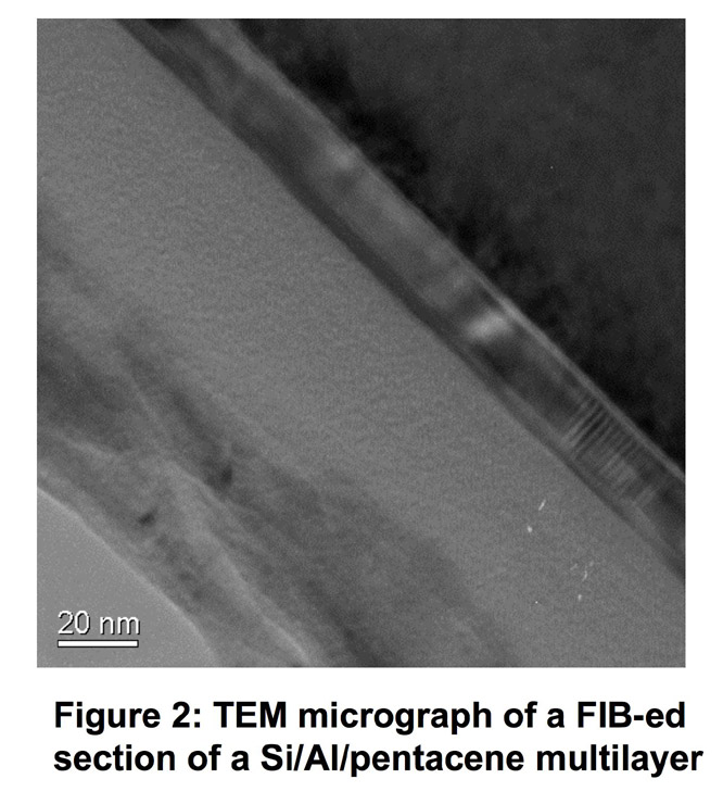
Nevertheless, we were able to make samples appropriate for TEM characterization
(Fig. 2). In the figure, the different layers are clearly visible. The
structure is Si, with a thin Al layer and a layer of pentacene. The TEM image
shows that the layers are clearly discernible and in spite of their vastly
different mechanical properties no decohesion takes place. Future work will
consist of characterizing the crystallinity of the pentacene layer in the TEM
sample as well as experimenting with other sample preparation methods such as
cryo-microtoming. If successful, the methods will be transferred to BHJ-type systems.

