

46713-B10
Exploring Defect Level Position and Occupation in Metamorphic Heterostructures for Multi-junction Photovoltaic Converters
Technological improvement of the conversion efficiency in state-of-the-art high efficiency solar cells depends, in part, on the development and refinement of high-bandgap alloys that can be grown on GaAs substrates. The bandgap in alloys like GaAsP and GaInP can be tuned to match design parameters that capitalize on the power available in the high-energy portion of the solar spectrum. However, the atomic spacing in these crystals differs from that of the underlying GaAs, so a higher concentration of crystalline defects is expected in GaAsP and GaInP epilayers. These defects impair solar cell performance by providing new pathways for photo-excited charge carriers to recombine rather than generate electricity.
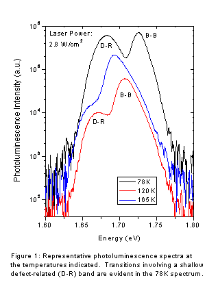
At I. Photoluminescence spectra from 1.75eV GaAsP
are shown in Figure 1. The broad
defect-related (D-R) peak below the band-to-band (B-B) emission indicates that
radiative recombination is occurring through relatively shallow defect levels
in this alloy. At higher temperatures
these transitions become nonradiative and, with increasing temperature, the
defect states become thermally depleted.
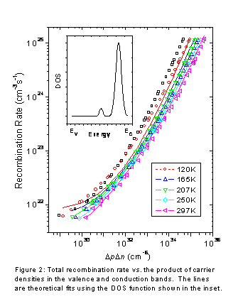
Analysis of the radiative efficiency (the radiative divided by the total
recombination rate) provides further evidence that a broad band of shallow
states exists in this material. Running
a rigorous computational algorithm to minimize the error between experimental
measurements and theoretical predictions of radiative efficiency vs. photo-excitation
produces the results shown in Figure 2.
The inset graph shows the computer-generated density of states (DOS)
distribution between the valence and conduction band edges (Ev
and Ec).
We find that a high density of defect levels just below Ec is required to obtain the best fit.
II. Transient
capacitance measurements on diodes during and after the application of a bias
pulse can be used to monitor the capture and emission of carriers into and out
of defect-related traps.
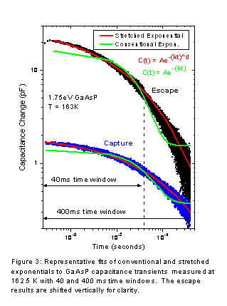 Representative
transients on devices incorporating 1.75eV GaAsP are shown in Figure 3. The capture and escape response deviates
strongly from conventional exponential behavior. Such non-exponential behavior is often
attributed to the presence of a broad band of defect energies, with shallow
levels emptying quickly at early times and slower deeper levels contributing at
later times. However, with
non-exponential behavior occurring during both the introduction and exclusion of
carriers from the depletion region, we assign the behavior to anomalous
transport rather than the filling and thermally-activated emptying of defect
states. For example, if carriers are
hopping between defect sites, quick motion would be expected between nearby
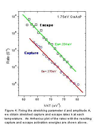
sites, while slower motion would occur during more distant hops. We fit the temperature-dependent response to
the stretched exponential function shown in the graph, holding the stretching
parameter d and amplitude A fixed. Arrhenius plots of the resulting capture and
emission rates (k) are linear and
yield comparable capture and escape activation energies (see Figure 4),
providing further evidence for the transport-limited interpretation noted
above. Indeed, we also observe a
thermally-activated, stretched-exponential response in 2.0eV GaInP, suggesting
that the simultaneous incorporation of Gallium and Phosphorous may be
responsible for this effect.
Representative
transients on devices incorporating 1.75eV GaAsP are shown in Figure 3. The capture and escape response deviates
strongly from conventional exponential behavior. Such non-exponential behavior is often
attributed to the presence of a broad band of defect energies, with shallow
levels emptying quickly at early times and slower deeper levels contributing at
later times. However, with
non-exponential behavior occurring during both the introduction and exclusion of
carriers from the depletion region, we assign the behavior to anomalous
transport rather than the filling and thermally-activated emptying of defect
states. For example, if carriers are
hopping between defect sites, quick motion would be expected between nearby
sites, while slower motion would occur during more distant hops. We fit the temperature-dependent response to
the stretched exponential function shown in the graph, holding the stretching
parameter d and amplitude A fixed. Arrhenius plots of the resulting capture and
emission rates (k) are linear and
yield comparable capture and escape activation energies (see Figure 4),
providing further evidence for the transport-limited interpretation noted
above. Indeed, we also observe a
thermally-activated, stretched-exponential response in 2.0eV GaInP, suggesting
that the simultaneous incorporation of Gallium and Phosphorous may be
responsible for this effect.
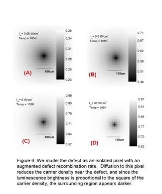
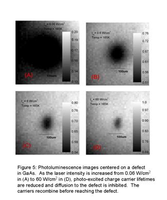 III. This summer, we undertook a new
experiment to image the photoluminescence generated by these materials using a
high-sensitivity CCD camera. We observed
striking spatial inhomogeneity in the luminescence
brightness, even in nominally lattice-matched GaAs. We also noted that the size of the
defect-related features depends strongly on the laser excitation intensity (see
Figure 5). At low density, carriers
diffuse more readily to defective regions rather than recombining radiatively, producing larger effective “dead” areas. We model the behavior by assigning a large
defect recombination rate to the defect position and allowing diffusion to
control the density of carriers in adjacent regions (see Figure 6). The results are consistent with our
observations, but a more sophisticated model will be required to achieve better
quantitative agreement with experiment.
At this stage, we can conclude that (1) if the defect recombination rate
is non-uniform throughout the sample, diffusion will contribute to a reduction
in net efficiency and (2) even for high-quality semiconductors with few
defects, diffusion can lead to significant defect recombination at low
excitation intensity. Preliminary images
from GaAsP grown lattice-mismatched on GaAs suggest that a hypothetical network
of defective pixels will be required to reconcile our diffusion-limited model
with experiment. Since the defect
concentration in these structures is much higher, we expect photo-excited
carriers to find defects more readily, raising the photo-excitation intensity
threshold for good solar cell performance.
III. This summer, we undertook a new
experiment to image the photoluminescence generated by these materials using a
high-sensitivity CCD camera. We observed
striking spatial inhomogeneity in the luminescence
brightness, even in nominally lattice-matched GaAs. We also noted that the size of the
defect-related features depends strongly on the laser excitation intensity (see
Figure 5). At low density, carriers
diffuse more readily to defective regions rather than recombining radiatively, producing larger effective “dead” areas. We model the behavior by assigning a large
defect recombination rate to the defect position and allowing diffusion to
control the density of carriers in adjacent regions (see Figure 6). The results are consistent with our
observations, but a more sophisticated model will be required to achieve better
quantitative agreement with experiment.
At this stage, we can conclude that (1) if the defect recombination rate
is non-uniform throughout the sample, diffusion will contribute to a reduction
in net efficiency and (2) even for high-quality semiconductors with few
defects, diffusion can lead to significant defect recombination at low
excitation intensity. Preliminary images
from GaAsP grown lattice-mismatched on GaAs suggest that a hypothetical network
of defective pixels will be required to reconcile our diffusion-limited model
with experiment. Since the defect
concentration in these structures is much higher, we expect photo-excited
carriers to find defects more readily, raising the photo-excitation intensity
threshold for good solar cell performance.