44403-G5
Synthesis of Inorganic Electrodes with Controlled Interfacial Structures by Crystal Engineering in Electrodeposition
(1) Synthesis
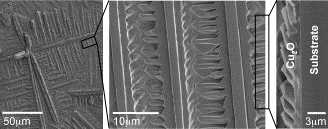
of Cu2O Electrodes Composed of Dendritic Crystals We have
demonstrated a new strategy of exploiting and manipulating dendritic growth of
Cu2O to produce photoelectrodes with high surface areas and good
electrical continuity. The
dendritic branching growth of Cu2O allowed for facile substrate
coverage and high surface roughness without growing a thick film. The resulting electrodes generated
significantly improved photocurrent compared to the electrodes composed of
micron-size faceted crystals that produced negligible short-circuit
photocurrent.
In order to
further enhance photocurrent, various methods to increase dendritic crystal
size were investigated. Increasing crystal size reduces crystal-crystal
boundary areas and ensures good electrical continuity in the larger domains of
the electrode. This can minimize
recombination losses and improve charge transport properties. Deposition potential, Cu2+
concentration, and acetate concentration were altered to regulate the
deposition overpotential, h,
which has a direct impact on nucleation
density and, therefore, on crystal size. Increasing crystal size consistently resulted in the
improvement of photocurrent regardless of the method used to regulate crystal
size. The electrode
showing the highest photocurrent was composed of dendritic crystals that
laterally expanded ca. 12000 mm2 while the thickness of the electrode was kept
below 5 mm (Figure 1).
This electrode generated more than 20 times higher photocurrent (0.45
mA/cm2) than the electrode containing the
smallest crystal size produced in our study with the average lateral size of
100 mm2 (0.02 mA/cm2). The
significant increase in photocurrent achieved simply by controlling the crystal
sizes in dendritic branching growth, without involving any compositional
changes, implies an enormous potential for morphology tailoring in improving properties of polycrystalline electrodes. (2) Synthesis of Highly
Transparent Nanocrystalline a-Fe2O3
electrodes Ferric
oxide (a-Fe2O3, hematite) is an n-type
semiconductor highly desirable for use in solar energy conversion due to its
bandgap (Eg = ~2.2 eV) that allows for utilizing the significant
portion of the solar energy spectrum. We have developed a new anodic deposition route to
prepare a-Fe2O3 electrodes using a
slightly acidic plating solution (pH 4.1). In this pH, Fe2+ ions are soluble without the
need of adding complexing agents, which simplifies the compositions of the
plating solution. Deposition in
this medium produced amorphous g-FeOOH films that can be
converted to highly transparent nanocrystalline a-Fe2O3
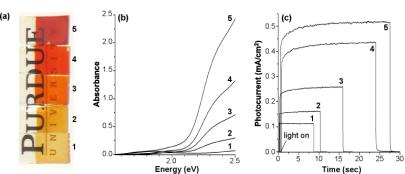
films by annealing. a-Fe2O3 films with
varying thickness were produced by changing deposition times in order to
investigate the effect of film thickness on photon absorption and photocurrent
generation. Films deposited for
1min, 2 min, 4 min, 8 min, and 16 min resulted in films with the average
thickness of 70 nm, 180 nm, 320 nm, 430 nm, and 680 nm, respectively, judging
from their cross sectional SEM images.
The photographs and UV-vis absorption spectra of the a-Fe2O3 films with
varying thicknesses are shown in Figure 2a-b. These films showed similar absorption features (i.e. onset
of band gap transition) but absorption increased gradually as the film
thickness increased.
The short-circuit photocurrent, which was measured
using a 60:40 solution of propylene carbonate: acetonitrile containing 0.5 M
tetrabutylammonium iodide and 0.04 M iodine, gradually increased as the film
thickness increased due to enhanced photon absorption and surface areas. However, when the film thickness
exceeds 460 nm, photocurrent decreased because severe aggregation of Fe2O3
particles at the Fe2O3/substrate interface increased
recombination losses in the film.