AmericanChemicalSociety.com
Reports: G10 48182-G10: Effects of Hydrogen-Surface Interactions on Photogenerated Electron Diffusion in Zinc Oxide Nanowires
The objective of our research is to study the interrelationship between impurity formation, surface state characteristics, and photogenerated charge carrier diffusion in ZnO nanowires.
During the current project period (September 1, 2009 to August 31, 2010), we have made important progress on revealing surface effects on photogenerated charge carrier diffusion, as well as the surface state characteristics as functions of the nanowire diameter, as described below.
In
our case, as LD is comparable to the optical aperture (~ 200
nm) of the NSOM probe, we approximated the optical field of the NSOM probe with
a Gaussian function and used an exponential-Gaussian convoluted function to fit
the spatial profile of IP, as shown in Figure 2. This
procedure allowed us to extract LD significantly smaller than
the NSOM probe size. Figure 3(a) shows measured LD (solid
circles) as a function of nanowire diameter. For nanowires with diameters larger
(smaller) than ~ 40 nm, LD exhibits a negligible (significant) diameter dependence. Particularly,
LD approaches ~ 250 nm as the diameter increases beyond 40
nm. This value is between 440 nm and 130 nm, which were reported for bulk
n-type ZnO with the doping levels of 1014 cm-3 and 1018
cm-3, respectively. As LD generally increases with
the decreasing electron concentration, we believe that LD
obtained for large-diameter nanowires (~ 250 nm) corresponds approximately to
the bulk value, considering that the electron concentration of ZnO nanowires is
~ 1017 cm-3. This absence of surface effects is
consistent with previous findings on bulk ZnO that surface states due to atomic
dangling bonds are resonant with conduction and valence bands, thus these surface
states do not For
carrier transport in nanowires with diameter smaller than 40 nm, surface
effects play an important role. The main mechanism of surface effects is the
carrier recombination via mid-bandgap surface states. To elucidate this, we
used a simple model based on carrier recombination mediated by mid-bandgap
surface states. In particular, with LD
given by (Dτeff)1/2,
where D and τeff are the diffusion constant (=kBTµp/q, with µp as the hole mobility) and the effective lifetime of
holes, respectively, the surface-mediated carrier recombination leads to a
decrease in τeff and
thus LD. This process can
be described by a simple model based on the continuity equation. With this, we
modeled LD as a function
of nanowire diameter [dotted blue line in Figure 3(a)]. A diameter-dependent
surface recombination velocity (S) is
required for a good fitting of the data using this model. The value of S ranges from ~ 1.5 × 10⁴
cm/s to ~ 0.1 cm/s as the diameter changes from 25 nm to 60 nm. At room
temperature, using a carrier capture cross section (σ) on the order of 10-15 cm2, we obtain
a surface state density (N) on the
order of 1011 cm-2 and 106 cm-2 for
25 nm and 60 nm diameter ZnO nanowires, respectively, as shown in Figure 3(b). To the best of our
knowledge, this is the first
experimental observation of a diameter-dependent surface electronic structure
in semiconductor nanowires, and this might be a universal phenomenon for many
semiconductor nanostructures. The increasing importance of surface effects, as
the material dimension shrinks, is commonly understood as a consequence of the
increasing surface-to-volume ratio. Our results suggest that, besides the surface-to-volume ratio, possible changes
in the surface electronic structures need to be considered in understanding
surface effects. Specifically for ZnO nanowires in solar cells, where the carrier transport is central to
energy conversion efficiency, our
 Using a scanning photocurrent
microscopy (SPCM) technique implemented on a near-field scanning optical
microscope (NSOM), with schematics shown in Figure 1 (a), we have obtained the
photogenerated hole diffusion length in individual n-type ZnO nanowires.
Particularly, the near-field photocurrent maps obtained by the SPCM technique
on a single nanowire Schottky diode, shown in Figure 1(b), exhibit a uniform
(highly localized) photocurrent spatial profile under the forward (reverse)-
biased condition. This is consistent with the rectifying electrical
characteristics of the Schottky diodes. Under the reverse-biased condition,
where the electric field is negligible in the nanowire except in the
space-charge region associated with the Schottky diode, the photocurrent is
induced by the collection of photogenerated holes (which diffuse from the
optical generation region under the NSOM probe) by the Schottky electrode. Only when the NSOM probe is within a short distance
(comparable or smaller than the hole diffusion length, LD)
from the Schottky electrode will such a photocurrent be detected. Therefore,
the decay of the photocurrent, IP, away from the Schottky
electrode, can be used to extract LD via a single exponential
relation, IP ~ exp (-x/LD).
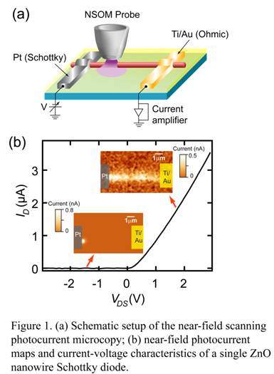
Using a scanning photocurrent
microscopy (SPCM) technique implemented on a near-field scanning optical
microscope (NSOM), with schematics shown in Figure 1 (a), we have obtained the
photogenerated hole diffusion length in individual n-type ZnO nanowires.
Particularly, the near-field photocurrent maps obtained by the SPCM technique
on a single nanowire Schottky diode, shown in Figure 1(b), exhibit a uniform
(highly localized) photocurrent spatial profile under the forward (reverse)-
biased condition. This is consistent with the rectifying electrical
characteristics of the Schottky diodes. Under the reverse-biased condition,
where the electric field is negligible in the nanowire except in the
space-charge region associated with the Schottky diode, the photocurrent is
induced by the collection of photogenerated holes (which diffuse from the
optical generation region under the NSOM probe) by the Schottky electrode. Only when the NSOM probe is within a short distance
(comparable or smaller than the hole diffusion length, LD)
from the Schottky electrode will such a photocurrent be detected. Therefore,
the decay of the photocurrent, IP, away from the Schottky
electrode, can be used to extract LD via a single exponential
relation, IP ~ exp (-x/LD). 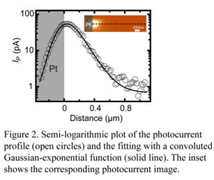 contribute
to carrier capture/recombination processes.
contribute
to carrier capture/recombination processes. 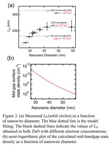 results
indicate that the surface passivation is only necessary for nanowires with
diameters smaller than 40 nm.
results
indicate that the surface passivation is only necessary for nanowires with
diameters smaller than 40 nm.
