AmericanChemicalSociety.com
Reports: UR10 50070-UR10: Controlling Morphology in Bulk Heterojunction Solar Cells via Chemical Design and Surface Patterning Methods
Lee Y. Park, PhD, Williams College
The ability to harvest more solar energy more efficiently (in terms of overall cost-of-implementation as well as quantum efficiency) is a critical challenge facing the scientific community. The development of organic solar cells promises to address several of the disadvantages of traditional solid-state based technologies. In particular, these offer the possibility of tailoring the absorption spectrum of the component materials, and of solution-processing light-weight, flexible, large area devices at low cost.
The
details of the micro- and nanoscale morphology that develop in polymer blend
films used in organic photovoltaic (bulk heterojuncction) devices play a
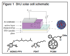
critical role in their performance. A schematic diagram of a BHJ solar cell is
shown in Figure 1. The "active
layer" is composed of a thin (~100 nm) phase-separated film of an electron
donating species (a soluble semiconducting polymer such as a PPV with a soluble
electron accepting species such as PCBM. Upon absorption of a photon, an exciton
is created which can then migrate within the film. At interfaces between donor and acceptor domains, the
exciton is separated into free holes and electrons. Under the influence of the inherent bias in the device
(created by the different conductive materials used as electrodes), these free
carriers can then travel to their respective electrodes. The details of the
microscopic phase separation that arises between the interpenetrating donor
(polymer) and acceptor (PCBM) networks in these films play a critical role in
device performance. The ideal
architecture is one in which light is absorbed efficiently, while at the same
time opportunities for exciton and free carrier recombination or annihilation
are minimized, thereby simultaneously optimizing charge generation, separation,
transport, and collection. Various
length scales are believed to be important in optimizing these different
aspects of device performance.
Optimal light absorption requires a polymer layer on the order of at
least 100 nm, while efficient charge separation requires a high interfacial
area between the donor and acceptor components, ideally with domain sizes comparable
to the exciton diffusion length (~10 nm) in order to minimize exciton recombination.
The most significant advances in performance achieved for these Our work thus far
has focused on the synthesis of new polyphenylenevinylene (PPV) type materials
containing fluorocarbon side chains.
We prepare our polymers via the commonly used base-catalyzed GILCH
polymerization (which gives rise to high MW PPVs), and have succeeded in
preparing a variety of new fluorocarbon-containing PPVs. Because of solubility
constraints encountered with these materials, we have thus far concentrated our
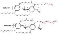
efforts on a series of random copolymers (of varying composition) of our
fluorinated monomers We have also begun investigating a
variety of possible strategies that might lead us to "blocky" copolymers. First, by starting with oligomers of
PPV as the monomers for the GILCH polymerization, we may be able to access
structures that have enough block-like character to further enhance the kind of
phase separation that is our goal.
Another possibility involves copolymerizations of GILCH monomers of
different reactivities as a means of preparing gradient polymers.
Finally, we have
also begun preliminary characterization of diode and photovoltaic behavior of
our fluorinated polymers, and are exploring the effect of different surface
chemistries on the transport properties of our polymer films.
 devices
in recent years are attributable to improvements in domain size and ordering
within domains. We are interested in exploring the use of
fluorocarbon-hydrocarbon interactions as a means of guiding and driving
organization and domain size within the active layer of this type of solar
cell.
 with
hydrocarbon analogs as illustrated here.
(Because the GILCH route is not a well-controlled polymerization, block
copolymers are unfortunately not accessible, as is typically the case for
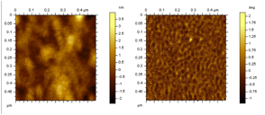
conjugated polymers.) Initial AFM
studies of these copolymers indicate that we may already be achieving enough
"blockiness" in our random copolymers to give rise to some phase
segregation. AFM images of thin
films one example of such a random copolymer are shown below: the films exhibit
a fine structure in the phase image (on the right) that is not
  visible
in the height image (on the left) that we attribute to some degree of
microphase segregation. In
addition, these materials exhibit an enhanced fluorescence (as compared with
hydrocarbon analogs) particularly in the solid state, further suggesting that
inclusion of the fluorinated side chains results in some form of enhanced
ordering.
Copyright © American Chemical Society

