AmericanChemicalSociety.com
Reports: DNI10 49187-DNI10: Control of Fundamental Length Scales in Polymer Solar Cells
 The aim of this project is to achieve simultaneously
an efficient absorption of photons with effective carrier extraction in Bulk-heterojunction (BHJ) solar cells; in standard flat cells
the two processes have opposing requirements.
Efficient absorption of light calls for thicker modules whereas carrier
transport always benefits from thinner ones.
Thus, this research work is directed specifically to address the disparate
length scales in polymer photovoltaic materials using photonic crystal
geometries. So far, we have obtained the following results:
The aim of this project is to achieve simultaneously
an efficient absorption of photons with effective carrier extraction in Bulk-heterojunction (BHJ) solar cells; in standard flat cells
the two processes have opposing requirements.
Efficient absorption of light calls for thicker modules whereas carrier
transport always benefits from thinner ones.
Thus, this research work is directed specifically to address the disparate
length scales in polymer photovoltaic materials using photonic crystal
geometries. So far, we have obtained the following results:
Physics and modeling of the polymer cell: It is essential to identify the correct electronic model for the BHJ cell since we will use such model as the framework to use a mathematical-optical optimization procedure to find the best photonic topology for the device. In particular, since the photonic crystal gets to be formed between the active polymer blend and its neighboring materials layers, understanding of the electronic impact of the neighboring layers is very important. The insertion of those additional layers between the photoactive layer and the electrodes have great impact in the device.
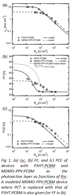
A) We have demonstrated that non-ideal series resistance
(Rsr) affects device performance differently depending on both the
strength and field dependence of the charge transfer (CT) states. This is
demonstrated by evaluating the Rsr J-V response for two BHJ systems,
poly(3-hexylthiophene) (P3HT) and
poly(2-methoxy-5-(3',7'-dimethyloctyloxy)-p-phenylene vinylene) (MDMO-PPV) each
combined with phenyl-C61-butyric acid methyl ester (PCBM). These two material
combinations represent extremes in BHJ behavior, where probability of splitting
the CT (PCT) state for P3HT:PCBM is 36% higher than
that for MDMO-PPV:PCBM at short-circuit and has a weaker electric field
dependence. Ultimately, this causes an increase in Jsc and
heightened sensitivity to Rsr. (see fig. 1, in particular part (a))
 B) We have shown
that light intensity measurements of devices with non-ideal Rsr and
Rsh (shunt resistance) are shown to convolute the scaling of both Jsc
and Voc. In particular, the Jsc dependence becomes
sub-linear under high Rsr, while the Voc deviates from
the usual logarithmic behavior for low Rsh.
B) We have shown
that light intensity measurements of devices with non-ideal Rsr and
Rsh (shunt resistance) are shown to convolute the scaling of both Jsc
and Voc. In particular, the Jsc dependence becomes
sub-linear under high Rsr, while the Voc deviates from
the usual logarithmic behavior for low Rsh.
C) We demonstrated the connection between the drift/diffusion and equivalent circuit model with regards to each model's treatment of PCT . In particular, the equivalent circuit model utilizes a light intensity dependent Rsh to describe the probability of splitting the CT and thus predicts a photocurrent under reverse bias that exceeds that permitted by light absorption.
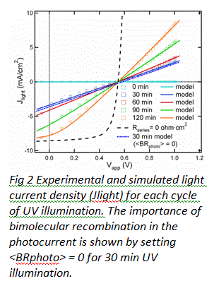
 D) We have found that tuning the electrical properties
of an electron transport layer (ETL) adjacent to the photoactive blend dictates
the range of Jsc and FF. An ETL such as TiOx, or ZnO are necessary
to operate the device by matching energy levels with the photoactive layer and
also to form photonic crystal structures. In particular, the UV sensitivity of
TiOx has been studied. We
observed that after UV exposure, Jsc improves by two orders of
magnitude while FF increases by a factor of three under solar simulated light.
UV exposure does not alter the device optical performance, Voc, or
the P3HT:PCBM electrical properties. Hence, both the micro- and macroscopic
electrical mechanisms that affect Jsc and FF upon insertion of an
additional layer can be probed. Through the use of device modeling and light
intensity experiments, we showed that an increase in the resistivity of the ETL
effectively turns on bimolecular recombination that is dominated by losses
related to the diode current in P3HT:PCBM. (Fig. 2)
D) We have found that tuning the electrical properties
of an electron transport layer (ETL) adjacent to the photoactive blend dictates
the range of Jsc and FF. An ETL such as TiOx, or ZnO are necessary
to operate the device by matching energy levels with the photoactive layer and
also to form photonic crystal structures. In particular, the UV sensitivity of
TiOx has been studied. We
observed that after UV exposure, Jsc improves by two orders of
magnitude while FF increases by a factor of three under solar simulated light.
UV exposure does not alter the device optical performance, Voc, or
the P3HT:PCBM electrical properties. Hence, both the micro- and macroscopic
electrical mechanisms that affect Jsc and FF upon insertion of an
additional layer can be probed. Through the use of device modeling and light
intensity experiments, we showed that an increase in the resistivity of the ETL
effectively turns on bimolecular recombination that is dominated by losses
related to the diode current in P3HT:PCBM. (Fig. 2)
Nanofabrication. We previously reported a route to fabricate scalable 2-D PC devices via a facile processing strategy called PRINT where enhanced performance was observed. However, the low efficiency resulting from a non-ideal BHJ system.
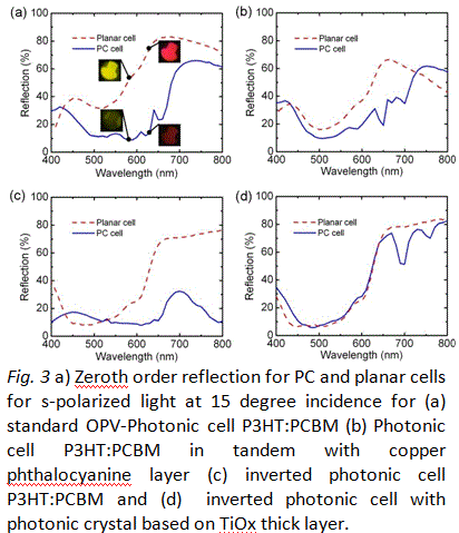
A) We have succesuflly fabricated 2-D PC OPV by using P3HT : PCBM, which has been widely used from the standpoint of an ideal BHJ morphology and high performance devices (fig. 3)
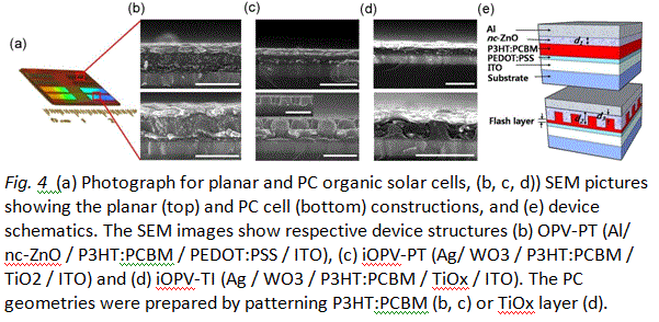
B) Also, we extend the fabrication technique to various device architectures for both inverted and standard OPV. (fig. 4) Furthermore, we demonstrate the flexibility of PRINT by presenting geometries of various nanopattern shapes and materials.
 Device performance for PC and planar control cells is
evaluated from both optical and electrical points of view. When absorption is
maximized for both PC and planar devices, an enhancement of 20% is possible. A
portion of this enhanced absorption comes in the form of resonant mode
excitations that are observed for many of the PC devices. Calculation showed
that the absorption by P3HT:PCBM in the PC cell was enhanced by about 43%
compared to the planar cells. In terms of device performance, the enhanced
absorption followed in the J-V measurement. Under 85mW/cm2 illumination, the
Jsc for PC (8.93 mA/cm2), was 40% higher compared to the planar cell
(6.36 mA/cm2), as shown in Figure 5C. This follows the absorption enhancement
predicted by the optical model. Finally, the acquired efficiency for the PC
cell is 2.91% with 0.61V open circuit voltage (Voc) and 46% fill
factor (FF).
Device performance for PC and planar control cells is
evaluated from both optical and electrical points of view. When absorption is
maximized for both PC and planar devices, an enhancement of 20% is possible. A
portion of this enhanced absorption comes in the form of resonant mode
excitations that are observed for many of the PC devices. Calculation showed
that the absorption by P3HT:PCBM in the PC cell was enhanced by about 43%
compared to the planar cells. In terms of device performance, the enhanced
absorption followed in the J-V measurement. Under 85mW/cm2 illumination, the
Jsc for PC (8.93 mA/cm2), was 40% higher compared to the planar cell
(6.36 mA/cm2), as shown in Figure 5C. This follows the absorption enhancement
predicted by the optical model. Finally, the acquired efficiency for the PC
cell is 2.91% with 0.61V open circuit voltage (Voc) and 46% fill
factor (FF).
