

45982-G10
Ultrafast Probing of Structures, Functions, and Pathways for Light-Excited Amorphous Silicon in Potential Energy Landscape
The main theme of the proposal is to investigate the structure-property relationship of various forms of amorphous silicon for photovoltaic application. The work proposed here is to enable the traditional ultrafast electron diffraction technique to characterize the photo-electric conversion efficiency following photoexcitation of amorphous silicon in its various amorphous states, from nanocrystalline to microscrystalline. Traditionally, the efficiency of a solar cell is characterized by determining the close-circuit photocurrent or open-circuit photovolatge of a solar cell. However, such measurement has never been conducted on the ultrafast time scale (picoseconds or less), required for characterizing the mechanism of carrier generations and transport to the interface in situ. We have recently developed a novel method to characterize the photovoltage based on ultrafst diffraction method, which also monitoring the relevant structures in which the photo-carrier generation is made. The basic idea behind this method is to monitor the shift of surface potential of the materials due to photo-carrier generation. In semiconductor, photovoltage is generated by modifying the barrier potential due to photo-induced redistribution of space charges near the interface. Such modification induces a Coulomb refraction effect on the coherently diffracted electron beams inside the materials. By following the diffracted Bragg interferences, we thus can identify the paths of electron beams and accordingly determine the corresponding changes of internal field which directly relates to the local carrier concentration in the diffraction monitored region, as demonstrated in Fig.1. This methodology has been tested in Si/SiO2 interfaces, where the coherent Bragg peaks are easily identifiable and the charge transfer into the surface states has been reliably characterized using time-resolved photoemission technique. Our transient photovoltage measurements performed on the timescale of 20ps to 3 ns coincide nicely with the dynamics of the surface carrier density, which controls the degree of charge separation and the inetrfacial potential at material junction under equilibrium condition. In the shorter time scale (1-30ps), we have revealed a regime of transient state in which the carrier dynamics does not follow the drift-diffusion equation completely. It is in this nonequilibrium regime that we can separate the diffusion from drift recombination, thus evaluating the transport characteristics of the space-charge region near the interface. Since the trap state serves as a recombination center, it plays an important role in determining the overall degree of charge separation and carrier lifetime, controlling the overall efficiency of a solar cell. These properties associated with a specific semiconductor materials can be determined using this novel contact-free diffractive potentiometry technique. Supported by PRF, we have further explored the dependence of the transient photovoltage on the energy, pulse-width, and fluence of the photoexcitation to explore the energy landscape of the charge injection/separation near the interface, in terms of local field (pulse-width dependent), distribution of charge-transferable states (energy dependent), and the mechanisms of charge injection through varying the carrier concentration (fluence dependent). Theory, which combines the Boltzmann transport and the drift-diffusion equation, is being developed to investigate these relevant hot carrier dynamics in this previously inaccessible ultrafast dynamical regime.
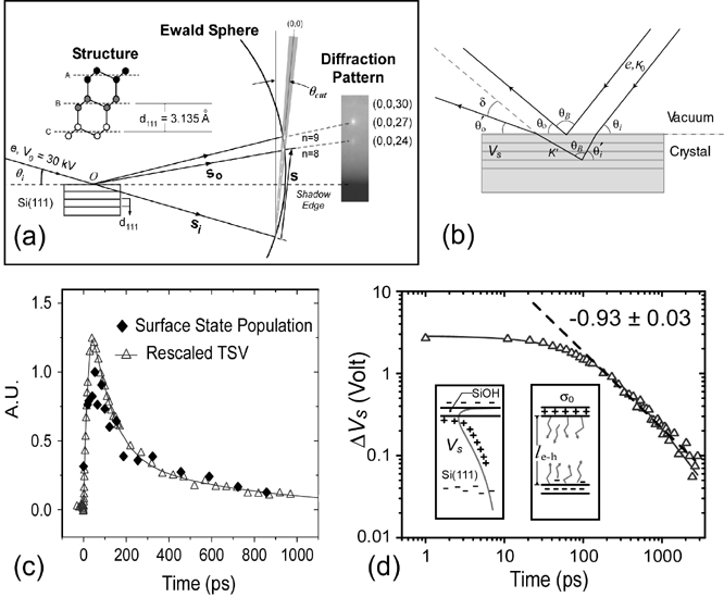
Fig.1. Ultrafast diffractive potentiometry approach for investigating photovoltage in nanostructures. (a) Electron diffraction geometry for studying a Si-111 interface. The diffracted beams (0,0,240, (0,0,27), (0,0,30) representing the coherently scattered electrons probing the surface of the Si-111 substrate. (b) Ray traces of the electron path with and without a surface potential (Vs) present. Vs induces a shift d in the diffraction maximum. (c) Transient surface-state population measured by photoemission compared to the measured TSV, demonstrating correlation of the surface state charging and the photovoltage. (d) Log-log plot of TSV exhibiting exponent –1 decay, which can be described by a drift-diffusion model of surface charge recombination.
In parallel, we also extended our structural determination method for ultrafast electron crystallography to include amorphous structures, especially to accentuate the embedded nanocrystalline structures, so as to access the different degrees of structural disorder in the commercially already implemented nanocrystalline, paracrystalline materials for solar cells. As demonstrated in Fig. 2, the nanoscale structural orders embedded within the continuous random network of amorphous silicon can be extracted using the diffraction difference method. 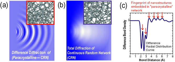
Fig.2. Structures of amorphous and paracrystalline silicon. The total patterns of amorphous structures, whether they are continuous random (CRN) or paracrystalline, are diffusive; while the difference pattern is distinctive of the minute nanoscale features of paracrystalline network in contrast to CRN. By performing Fourier analysis of the ‘difference pattern’, the ‘difference radial distribution curve’ is obtained. Panel (c) clearly shows the change of local orders in terms of periodic depletion and formation of bonds between 2—7 Å.
Our further effort will involve combining both methods for amorphous silicon study.