
Back to Table of Contents
44228-G5
Studies of Interface Structure and Properties of Thin Films
Theodosia Gougousi, University of Maryland (Baltimore County)
The atomic layer
deposition of HfO2 thin films is studied on GaAs(100) surfaces. GaAs
substrates exhibit higher carrier mobility than Si substrates and as a result
are considered as possible materials for advanced electronic devices. Two
different chemistries that utilize Hf-amide precursors were investigated: i) tetrakis(dimethyl)amino
hafnium (TDMAHf) and H2O at a deposition temperature of 275°C and ii)
tetrakis(ethylmethyl)amino hafnium (TEMAHf) and H2O at a deposition
temperature of 250°C. Several GaAs starting surfaces were investigated,
including native oxide and both HF and NH4OH-treated substrates. Wet
chemical etching in either HF or NH4OH solutions are shown to remove
most of the Ga and As native oxides (Figure 1).
i)
TDMAHf + H2O: For the TDMAHf process spectroscopic
ellipsometry (SE) confirms linear growth rates of ~1.1 Ĺ/cycle for all
surfaces. Rutherford backscattering spectrometry (RBS) shows that deposition
on the surface native oxide results in very smooth growth of ~ 2.9×10¹⁴
Hf/cm2/cycle. For the HF and NH4OH-etched GaAs surfaces
steady state is reached after 10 ALD cycles with comparable growth rates
(Figure 2). The interface of HfO2 films deposited on GaAs surfaces
is probed by X-ray photoelectron spectroscopy. Both the HF and NH4OH
treatments passivate the surface and prevent the oxidation of the interface
during the deposition of coalesced HfO2 films (> 15 ALD cycles)
(Figure 3). Deposition of HfO2 films on the native oxide GaAs
surfaces show gradual consumption of the native oxides during the process,
indicating the presence of an “interfacial cleaning” mechanism comparable to
that observed for other ALD processes.[1],[2],[3],[4]
The As-oxide and most of the Ga-oxide is completely removed after 20 ALD
cycles. The presence of As oxides is not detected for films as thick as ~100Ĺ
(100 cycles) deposited on native oxide substrates (Figure 4).
ii)
TEMAHf + H2O: A similar to the previously observed
interface cleaning reaction is observed for deposition on GaAs native oxides.
The oxide consumption reaction appears to be proceeding somewhat slower as it
requires ~25 cycles for complete removal of the interface oxides compared to
~20 cycles for the TDMAHf process (Figure 5). A possible explanation if this
slower reaction is confirmed is through a difference in the ALD mechanism for
the two precursors. In the case of the TDMAHf precursor the ALD reaction can
only proceed through reduction of the ligands but for TEMAHf an additional
pathway may be possible through beta hydride elimination.[5]
If this secondary path is accessible it is almost certain it will produce
different products than the reductive path. These "different" products
may not react as efficiently with the Ga and As native oxides. We are currently
investigating this effect in more detail including RBS surface coverage
measurements.
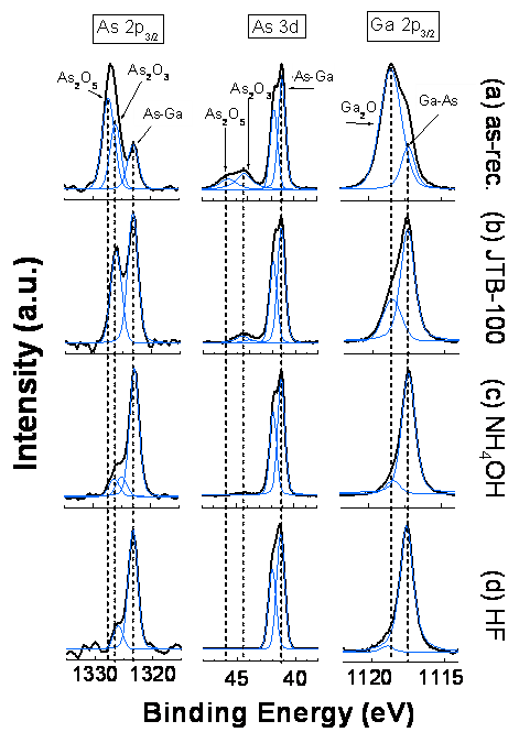
Figure 1: XPS scan of the As 2p, As 3d and Ga
2p regions for different GaAs surfaces: (a) native oxide, (b) cleaned in
JTB-100, (c) etched in 30% NH4OH aqueous solution and (d) etched in
HF solution.
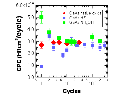
Figure 2: Hf atom surface
coverage per ALD cycle as measured by RBS for the TDMAHf + H2O
chemistry. The three starting surfaces are surfaces (a), (c) and (d) from
Figure 1.
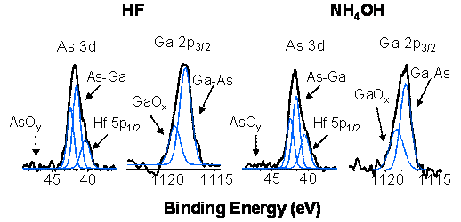
Figure 3. Deposition of
~15 Ĺ of HfO2 using the TDMAHf + H2O chemistry on HF and
NH4OH etched GaAs surfaces does not cause regrowth of the native
oxides indicating surface passivation.
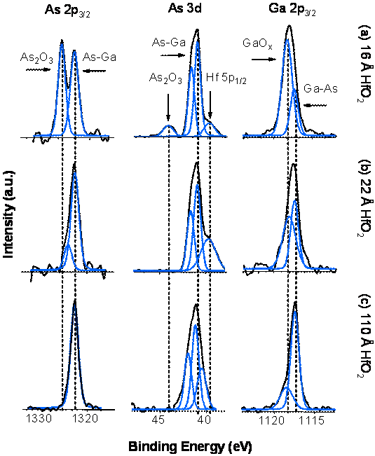
Figure 4. Gradual
consumption of the surface native oxides is observed during the deposition of
HfO2 films from TDMAHf and H2O on cleaned GaAs native
oxide surfaces.
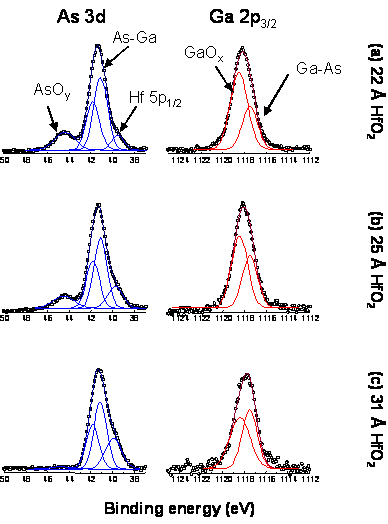
Figure 5. Gradual
consumption of the surface native oxides is observed during the deposition of
HfO2 films from TEMAHf and H2O on cleaned GaAs native
oxide surfaces. The film thickness is based on growth rates measured on native
oxide Si surfaces. RBS surface coverage measurements will be performed to allow
a direct comparison between the data on Figures 4 and 5.
[1]
M.M. Frank, G.D. Wilk, D.
Starodub, T. Gustafsson, E. Garfunkel, Y.J. Chabal, J. Grazul, D.A. Muller,
Appl. Phys. Lett.
86, 152904 (2005)
[2]
M.L. Huang, Y.C. Chang, C.H. Chang, Y.J. Lee, P.
Chang, J. Kwo, T.B. Wu, M. Hong, Appl. Phys. Lett.
87, 252104 (2005)
[3]
C.-H. Chang, Y.-K. Chiou, Y.-C. Chang, K.-Y.
Lee, T.-D. Lin, T.-B. Wu, M. Hong, J. Kwo, Appl. Phys. Lett. 89, 242911
(2006)
[4]
D. Shahrjerdi, E. Tutuc, S.K. Banerjee, Appl.
Phys. Lett. 91, 063501 (2007)
[5] F. Zaera, Francisco
Zaera, J. Mater. Chem., 2008, (Advance Article)
Back to top
