ACS PRF | ACS
All e-Annual Reports

43352-G5
Conductive-Probe AFM Evaluation of Nanopatterned Metal-Molecule-Metal Junctions Fabricated via Electroless Metal Deposition
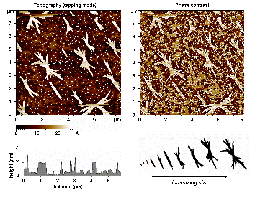
Advancement of molecule-based electronic systems will require the ability to achieve reliable and precise measurements of conductance and charge transport for nano-sized molecular test structures. A considerable challenge is posed for developing effective, reproducible methods for measurements in nanosized systems, for scaling molecular electronic devices to nanometer length scales, and for systematically evaluating the effects of molecular structure on electrical properties. This proposal aims to develop and pioneer new methods for the controlled assembly of molecules such as porphyrins using surfaces as an architectural template. Conceptually, by arranging and orienting porphyrins on well-defined surfaces, local measurements of charge transport can be enabled for different pathways through the molecules. Accurate and precise electronic property measurements will shed insight on the fundamental mechanisms that give rise to properties such as resistance and rectification with changes in chemical structure. Fundamental understanding of the interactions of molecules binding to substrates for forming robust 3D assemblies is essential for developing workable technologies for molecular electronics. Studies (CP-AFM) with designed molecular test platforms of porphyrin assemblies will be compared to theoretical models of charge transfer and electronic properties, and correlated to the structure of porphyrin molecules. Nanofabricated test platforms of ů-functionalized n-alkanethiol self-assembled monolayers will be used as architectural templates to guide the deposition of porphyrins with controlled orientation. The overall impact of this work is to develop new strategies for the preparation of porphyrin thin films for highly local measurements and surface characterizations; to measure the conductive properties of porphyrin architectures using designed molecular test structures; and to begin to develop theoretical models for predicting transport properties in porphyrins, based on experimental measurements. Porphyrins provide an excellent model system to determine the effects of various peripheral groups on the macrocycle as well as to determine how coordinated metals influence the organization and properties of porphyrin nanostructures. Due to their photophysical properties, porphyrins can be applied for sensors, photonic devices, photovoltaic cells, molecular switching and memory devices. Experimental results using AFM and conductive probe measurements can be used comparatively for deriving predictive models of electron transport in designed assemblies. The goals include developing viable chemical strategies for immobilizing and linking porphyrins to surfaces with maximized attributes (stability, properties) for electronic device designs. We have found that the successive evolution of the stages of crystal growth of porphyrin-cobaltacarborane conjugates in solution can be viewed using AFM snapshots at various intervals of incubation. (Chem. Eur. J., 2007) The example images display changes in morphology with increasing sizes of aggregates. The smallest structures are the spherical seed particles, which begin to organize into linear and then columnar shapes. The linear columns then grow larger by assembling laterally into rectangular 2-D sheets. As the sheets become larger, branching takes place from the centers of the planar sheets. The thickness of the bright structures within the figure corresponds to the dimensions of a single layer of porphyrins. The heights of the sheets and nanocrystals are identical, suggesting that in solution the porphyrin crystals grow through assembly at the edges of the sheets in a planar, 2-D direction. Progress has been gained for preparing nanosized test junctions for metal-molecule-semiconductor heterojunctions. Particle lithography was used to prepare arrays of nanostructures for measurements with current-sensing AFM. Simultaneously acquired topography and current images (-5 V bias) are shown for samples of octadecyltrichlorosilane (OTS) nanopatterns with iron oxide deposits. The results display representative I-V profiles for the nanoscale test platform. Very little current is measured for the insulator OTS molecules, however the current image acquired at -8 V bias selectively maps the areas of conduction between rings (bright contrast). The onset of current occurs at -6 V and +10V for the metal contacts of the metal-molecule-semiconductor junctions, and the current image shows conduction (bright contrast) for the metal deposits. Nanostructured surfaces enable comparisons of different materials or molecules within the same experimental platform, for purposes of internal calibration. For example, when conductive molecules are patterned within an insulating matrix SAM, the matrix provides an internal reference standard. We have discovered that pyridyl-substituted porphyrins naturally self-assemble into continuous films of monolayer thickness on surfaces of Au(111) with a co-planar orientation. (manuscript in preparation). The adsorption is likely mediated through N-Au chemisorptive linkages. Scanning probe lithography can be applied with the pyridyl-porphyrin films, both nanografting and nanoshaving protocols have been successful. The films of pyridyl porphyrins provide a stable matrix layer for nanografting patterns of n-alkanethiols, without evidence of exchange reactions. When pyridyl porphyrins are nanografted within n-alkanethiol self-assembled monolayers, spatial constraint causes a different surface assembly process; the patterns form a standing orientation with heights corresponding to an upright configuration. Thus, pyridyl-substituted porphyrins provide a convenient model system for studies of conductance and photonic properties, with inherent advantages of robust molecular architectures resistant to thermal and oxidative degradation.