www.acsprf.org
Reports: DNI1049952-DNI10: Photocarrier Generation and Multiplication in Carbon Nanotubes
Introduction
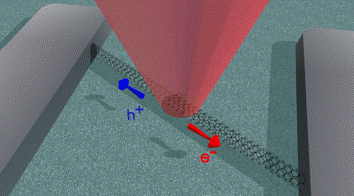
We have built a scanning photocurrent microscope (SPCM) with high spatial and spectral resolution and have used this instrument to investigate the photocurrent generation process in carbon nanotube (CNT) devices. Figure 1 illustrates the general principle of our measurements. Electron-hole pairs are generated by a tightly focused laser and driven toward metal electrodes by built-in electric fields. The center of the laser spot is controlled with 10 nm resolution and the wavelength of the laser is continuously variable between 450 nm and 1800 nm.
In our first measurements we investigated CNT devices in ambient conditions with CNTs on oxide surfaces. However, the room temperature oxide surface was unsuitable for our measurements. The charge groups on the oxide surface made it impossible to establish stable doping levels and stable built-in electric fields.
Experimental highlights from the reporting period
Figure 2 shows the suspended CNT geometry that we designed and fabricated to overcome the issues associated with device stability. The CNT is grown as the last step of the fabrication process. The CNT bridges the gap between a pair of Pt electrodes. The Raman spectra from the CNT shows no defect peak at 1350 cm-1, indicating an extremely clean CNT.
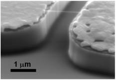
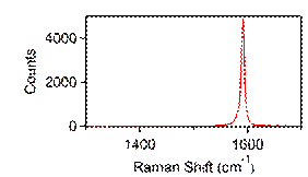
Figure 3a shows the intensity of reflected light from a suspended CNT device. Reflected light from the Pt electrodes are clearly visible. Figure 3b shows the photocurrent that is generated as the laser scans over the device. There is no voltage bias applied to the device. The strong photocurrent signal at the CNT-Pt contacts corresponds to the built-in electric fields at the metal-semiconductor interface.
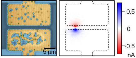
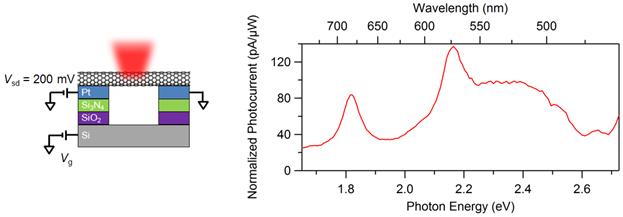
Figure 4 shows spectrally resolved photocurrent from a semiconducting CNT. A bias voltage was applied between the Pt electrodes to drive the electron-hole pairs out of the CNT. With this geometry we were able to detect photoabsorption resonances associated with the CNT band structure. The peaks at 1.82 eV and 2.17 eV are a spectral fingerprint that is determined by the chiral index of the CNT and the strength of electron-electron interactions in the CNT.
Next steps
The project has reached a point where we can begin investigating the efficiency of the photogeneration process as a function of photon energy, dielectric environment and electric field strength. We plan to begin measurements of suspended CNT devices at different electric fields, and with and without dielectric coatings.
Impact on career
Preliminary data taken from the SPCM microscope was the foundation for my NSF CAREER award application (submitted July 2011). The SPCM has also given my lab a unique advantage in the field of nanometrology, leading to collaborations with Prof. Oksana Ostroverkhova (OSU) and Prof. George Nazin (UO).
Impact on students
Tristan DeBorde (PhD candidate at OSU, Physics) and Rachel Burton (undergraduate physics major at OSU) have been supported by the research funds. Tristan began working on the project in Jan 2010 and has become an expert in the field of opto-electronics with carbon-based nanodevices.