www.acsprf.org
Reports: ND1048813-ND10: Renewable Energy from a Neglected Photovoltaic Material: Boron Arsenide
Boron arsenide has been synthesized via the reaction of elemental boron with an excess of elemental arsenic in sealed, evacuated quartz tubes heated to 800 degrees C for twelve hours. The reaction of molar equivalents of boron and arsenic under similar conditions has been reported previously.1 However, in our experiments it was found that the reaction of equimolar quantities of these elements resulted in the production of a material that is deficient in arsenic. Subsequent systematic variation of the boron to arsenic mole ratios revealed that it is necessary to use a 2:1 arsenic to boron mole ratio in order to produce a material with the desired one-to-one stoichiometry.
Recently, large pieces of boron ranging in size from 0.4 to 4 mm were allowed to react with two molar equivalents of arsenic under similar conditions to those described above. Scanning electron microscopy images, which are displayed in Figure 1, revealed that an interesting surface reaction took place, resulting in the deposition of a thin layer of boron arsenide on top of the boron surface. The thin layer is not continuous and features gaps where the boron core is clearly visible. The presence of polycrystalline boron arsenide and elemental boron were established on the basis of X-ray powder diffraction data taken from a single piece of the material. X-ray photoelectron spectroscopy was performed to analyze the chemical composition of the new boron arsenide material. The high resolution spectra shown in Figure 2 revealed a 1:1 atomic ratio of boron and arsenic, confirming the materials composition.
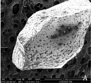
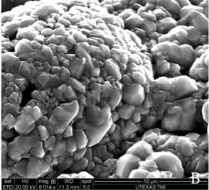
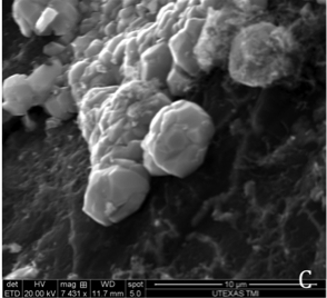
Figure 1. SEM images reveal the surface and core structure of the material produced by the thermal reaction of 0.4 to 4 mm boron pieces and two molar equivalents of arsenic. (A) Single piece of the new material. (B) Area of continuous BAs surface coverage. (C) Area featuring gap in surface coverage. Light material is BAs, dark material is boron core.
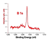
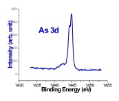
Figure 2. High resolution XPS spectra of boron arsenide material.
A gold layer approximately 200 nm in thickness was deposited on one side of a single piece of the new boron arsenide material. This was accomplished using a special gold alloy electroplating solution (SG-50. Transene Co., Inc., Rowley, MA) as the working solution in a two electrode system by applying a potential at -1.0 V. A silver epoxy was used to connect the wire to the gold layer. Silicone gel was used to cover the silver epoxy and wire, resulting in a boron arsenide electrode with an active surface area of 1 mm2, as shown in Figure 3.
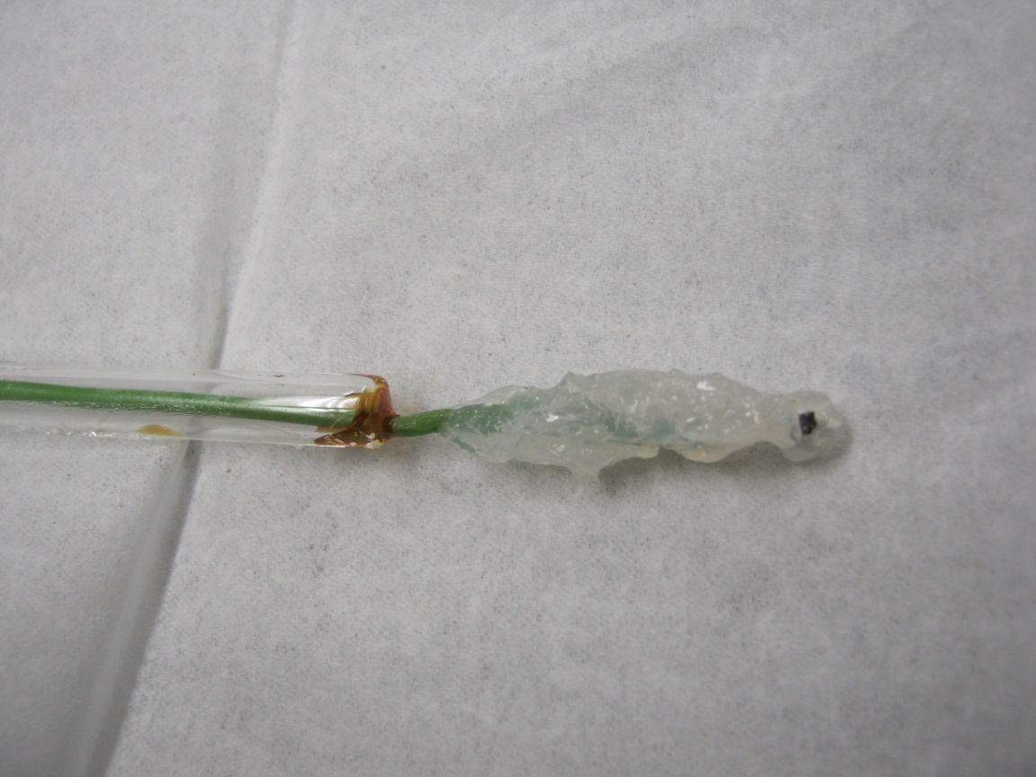
Figure 3. The boron arsenide electrode.
The newly synthesized boron arsenide material displays p-type behavior and is active under both visible and UV light irradiation, as shown in the linear sweep voltammograms in Figure 4. The measured photocurrent, displayed in Figure 5, is approximately 0.1 mA/cm2 at an applied potential of -0.25 V vs. Ag/AgCl under full xenon lamp irradiation.
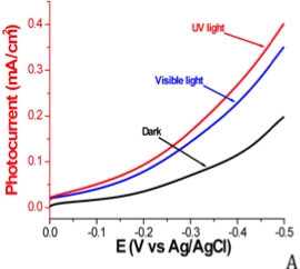
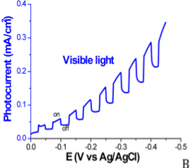
Figure 4. Linear sweep voltammograms of boron arsenide material in 0.01 M methyl viologen with 0.1 M Na2SO4. Potential is swept from 0.0 V to -0.5 V vs. Ag/AgCl at a scan rate of 10 mV/s using a 100 mW/cm2 Xe lamp. (A) Photocurrent of the new boron arsenide material in the dark, under visible light irradiation, and under UV light irradiation. (B) Chopped photocurrent under visible light irradiation. (C) Chopped photocurrent under UV light irradiation.
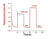
Figure 5. Photocurrent at an applied potential of -0.25 V vs. Ag/AgCl in the dark (0-20 s, 40-60 s, and 80-100 s), under visible light irradiation (20-40 s), and under UV light irradiation (60-80 s).
Two new types of experiments are anticipated in the near future. The first such experiment will feature the use of larger pieces of boron that range in size from 10 to 30 mm. It is hoped that the reaction of the larger pieces of boron with two molar equivalents of arsenic will result in the deposition of an increased area of continuous boron arsenide surface coverage that will enable more precise photoelectrochemical studies. The second new experiment will feature the use of boron particles in the nanometer size range. It is anticipated that the reaction of these nano boron particles with two molar equivalents of arsenic will permit exploration of the effect of increasing the surface to core ratio.
Alternative methods of preparing boron arsenide are being explored continuously. For example, the synthesis of a small molecule that features alkyl ligands and sigma-bonds between boron and arsenic is being evaluated at the present time. The alkyl ligands are expected to be thermally labile and undergo beta-hydride elimination in a fashion that has been demonstrated previously.2 The robust sigma-bonds between boron and arsenic are expected to promote stoichiometric control of the elimination reaction. Once the precursor has been synthesized, boron arsenide film growth by thermal decomposition of the precursor will be explored via chemical vapor deposition.
- Perri, J. A.; La Placa, S.; Post, B. Acta Crystallogr. 1958, 11, 310.
- Miller, J. E.; Kidd, K. B.; Cowley, A. H.; Jones, R. A.; Ekerdt, J. G.; Gysling, H. J.; Wernberg, A. A.; Blanton, T. N. Chem Mater. 1990, 2, 589-593.