www.acsprf.org
Reports: DNI1049790-DNI10: Harnessing Surface Plasmon Subwavelength Optics in Metallic Nanostructures for Enhanced Efficiency in Thin-Film Solar Cells
In the second year, the PI's team has developed new techniques for engineering metallic nanostructures and also demonstrated high-performance, nanostructured plasmonic electrodes integrated with organic photovoltaic cells. This work has led to multiple papers in scientific journals as well as presentations at conferences and academic institutions.
The goal of this DNI project is to develop low-cost processing techniques for engineering nanostructured metal films as semi-transparent electrodes to improve the optical absorption and power conversion efficiency of thin-film solar cells. As it was described in the original proposal, our team employed nanosphere lithography (NSL) techniques to produce self-assembled, centimeter-sized plasmonic electrodes patterned with nanohole arrays. Following a series of design optimization via computer modeling and optical characterization, in Year 2, these plasmonic electrodes have been integrated with organic photovoltaic cells.
We have performed systematic computer simulations using 3-D finite-difference time-domain (FDTD) methods. To improve the accuracy of our modeling, we have performed ellipsometry to measure dielectric constants of the materials, i.e. Ag film with varying thicknesses (Fig. 1; left) as well as each constituent layer of organic photovoltaic cells. Subsequently, we have performed a series of 3-D simulations to map the field distribution inside OPV cells (Fig. 1; right) with a regular ITO electrode vs. plasmonic Ag electrodes.
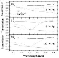
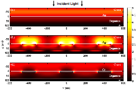
Fig. 1. Optical characterization and computer modeling of nanoplasmonic Ag electrodes. (Left) Measured transmission spectra for ITO, (a) 12 nm, (b) 16 nm and (c) 20 nm Ag films on a glass substrate. The transmission increases uniformly with decreasing Ag thickness and spectral features arise due to patterning. Patterned films exhibit a dip and a peak in the transmission due to the excitation of surface plasmons. (Right) Simulated cross-sectional field intensity maps at l = 622 nm. The anode is varied to demonstrate the difference in plasmonic enhancement for (a) 12 nm unpatterned Ag, and (b) 12 nm patterned Ag having 250 nm holes with a periodicity of 400 nm and (c) a similarly patterned Cr anode. The difference between (a) and (b) demonstrates the presence of a plasmonic response with patterning. A comparison of (b) and (c) shows the disparity in field enhancement between a metal that supports surface plasmons (Ag) and one that is extremely lossy (Cr).
Subsequently, these nano-patterned Ag electrodes were integrated with OPVs in collaboration with Prof. Russell Holmes (UMN Chemical Engineering) (Fig. 2).
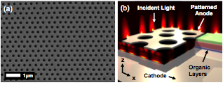
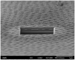
Figure 2. (a) Top-down SEM image of the patterned Ag electrode; (b) 3-D schematic of our plasmonic OPV cell; (c) cross-section SEM image of the integrated OPV cell. The bright region in the cross-section correspond to the 12-nm-thick Ag film with periodic nanohole patterns.
As summarized in Fig. 3, the integrated plasmonic OPV cells showed performance equal to that of an ITO-based reference cells, accomplishing our goal to demonstrate centimeter-sized low-cost plasmonic electrodes that can boost the power conversion efficiency in thin-film solar cells. While there have been many attempts to integrate patterned Ag-nanostructures into OPVs for enhanced absorption, the majority of previous reports have shown device efficiencies below those for cells constructed using a conventional ITO anode because of the use of relatively thick metal films and/or a polarization dependence when one-dimensional grating structures are used. We believe that our work is unique since it demonstrates that the solution-based nanosphere lithography technique can be scaled to larger area at a practical cost, and also show performance equal to that of ITO-based architecture. Furthermore, the NSL technique used here can be easily practiced by many other researchers, which will facilitate broad dissemination of this architecture to the plasmonic OPV community and is likely to provide real advantages in practical implementation.
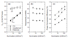
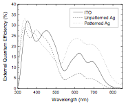
Figure 3. Device performance parameters under AM1.5G simulated solar illumination. (a) Comparable values for the open-circuit voltage (VOC) and fill factor (FF) are obtained using all anodes, demonstrating comparable electrical performance. (b) Devices with a patterned anode show the highest responsivity due to the plasmonic field enhancement. (c) The increased responsivity of the patterned device leads to a higher power conversion efficiency relative to devices using either an ITO or unpatterned Ag anode. External quantum efficiency (ηEQE) for devices with anodes consisting of ITO, and 12 nm unpatterned and patterned Ag. The ηEQE increase for devices with a patterned anode at wavelengths larger than 500 nm reflects the enhanced absorption in the CuPc donor arising from spectrally-broad plasmonic contributions at the anode-donor interface. Adapted from Luhman et al., Appl. Phys. Lett. (2011). [4]
In addition to plasmonic nanohole electrodes, we have also investigated metallic grating structures (i.e. bumps and grooves patterned in Ag films) for light harvesting. We employed another new fabrication technique, called template stripping, to make high-quality Ag films (Fig. 4). By varying the geometry of Ag plasmonic gratings with 1-2 nm precision, we are now able to systematically study how small changes in the geometry affects light coupling efficiency, which will allow us to further optimize the plasmonic electrode designs in the future.
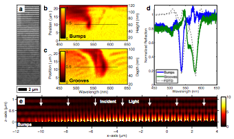
Figure 4. a, SEM image of a ramped and chirped Ag grating. Within the grating, the height and spacing of the bumps is finely tuned for maximizing the surface plasmon generation efficiency. b, Reflection map of the grating. The vertical axis represents space, or position along the grating, and is labeled with the corresponding bump height and period. The horizontal axis represents wavelength, and the data is normalized to the reflection of light polarized parallel to the grating lines, where surface plasmons are not excited. The central dark regions incidate the generation of surface plamons. c, Similar results were obtained for a ramped and chirped grating of grooves. The horizontal dashed line shows d, a cross-section through the minimum of reflectivity. The sharp reflectivity dips indicate a well-tuned grating, corroborated with FDTD simulations. e, Visualizing the total electromagnetic field in the bump grating verifies that surface plasmons are efficiently excited only for a certain range of bump heights.