www.acsprf.org
Reports: ND949302-ND9: Bubble Detachment on Micro/Nano Structured Solid Surfaces in Energy Applications
The goal of this project is to develop a new method to enhance bubble detachment and to investigate the detachment mechanism. A key idea is to engineer micro/nano structured surfaces. In this second year, our efforts have been mainly focused on developing and manufacturing nanostructures surfaces. Investigating of the nano fabricated surfaces for bubble detachment will be carried out in this third year (note that this project has been no-cost extended until August 31, 2012). In the second year, we have developed a tunable two-mirror interference lithography system that can significantly increase the nano-patterning area with great controllability of pattern periodicity [2, 3].
A Lloyd-mirror interferometer consists of a mirror attached perpendicular to a substrate, where a simple angular rotation of the device allows a convenient control of pattern periodicity. However, the effective pattern coverage area is significantly dependent on a mirror size and an optical coherence length [1]. This year we have studied and developed a new IL system featuring two rotational mirrors, which result in both the tunability in pattern periodicity and the large-area pattern coverage effectively [2, 3]. Figure 1 displays the schematic of the new IL system. A laser beam is first split into two beams and expanded by spatial filters. As opposed to the conventional two-beam system, a rotational mirror is introduced in the path of each expanded beam and independently regulated to an arbitrary angle (b). Combined with the translational sample stage along an optical rail, the incident angle of a mirror-reflected light to the substrate (q) is then freely adjustable for a desirable pattern period without the need of an optical path reconfiguration. Such configuration allows the system to occupy less space than the conventional two-beam system, since the rotating mirrors are capable of providing the necessary degrees of freedom. Additionally, such flexible configurability does not require an increase of the expanded beam path distance in producing different pattern periodicities so that a relatively low power laser can still maintain a high throughput.
1-D nanograting patterns were fabricated for various periodicities on 4-inch silicon substrates by using a 50 mW HeCd laser (λ = 325 nm, coherence length = ~30 cm) and 4-inch mirrors. The laser beam (Fug. 1) was split into two by a dielectric beam splitter. Both transmission and reflection beams were incident into spatial filters with the same optical path length and expanded over 1.6 m to guarantee a uniform Gaussian intensity distribution (greater than 80% with the FWHM of 6 inches) over the 4-inch mirror surface. Each mirror was assembled on a rotation stage and redirected the expanded beam to a sample stage set along an optical rail. For a photoresist layer, negative resist (NR7-70P, Futurrex) was spin-coated on the silicon substrate to a film thickness of 100 nm, and soft-baked at 150 ¼C for 1 min. After exposure, the sample was post-baked at 100 ¼C for 1 min and developed by RD6 (Futurrex).
Figure 2 shows the experimental results for three different periods, 250, 500, and 750 nm. The incident angle (θ) for each period was regulated at 40.5¼, 19.0¼, and 12.5¼, respectively. The visible diffraction colors spanning over the whole wafers indicates uniform coverage of the nanostructures on the substrates. Scanning electron microscope (SEM) measurements further verify that the nanopatterns are well-defined and uniform over the entire wafer area (less than 10% variation in line width and edge roughness) regardless of the pattern periodicities. The uniform nanopatterns over the whole 4-inch wafer confirm the feasibility of the new IL system for tunable periods while retaining the large coverage area.
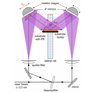
Figure 1. Schematic of a two-mirror IL system with geometrical parameters of tunable components.
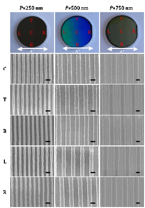
Figure 2. Fabricated 1-D nanograting patterns at different periods. Three columns from left to right correspond to the periods of 250, 500, and 750 nm, respectively. Symbols 'C', 'T', 'B', 'L', and 'R' represent five different locations on the 4-inch wafers for the SEM measurements. A scale bar in each SEM image represents 250 nm.
The new IL system was then employed to engineer various high-aspect ratio 3D nanostructures [3]. Nanostructures up to 1 μm tall and with the aspect ratio of 1:8 were realized (Figure 3). Such well-regulated thick PR mask layer further allowed us to transfer the patterns onto other substrates to define high-aspect-ratio 3D nanostructures with a wide range of substrate materials (Figure 4).
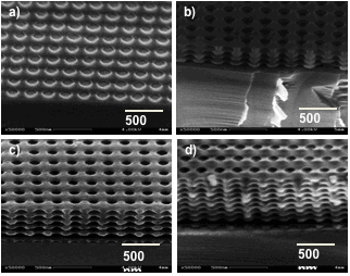
Figure 3. Scanning electron microscope (SEM) images of varying aspect ratios (ARs) of PR nanopore patterns with a constant periodicity of 250 nm. a) AR=1:1. b) AR=1:3. c) AR=1:5. d) AR=1:8.
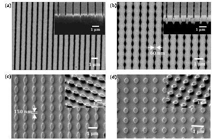
Figure 4. Variation of pattern shapes. (a) Linear line pattern. (b) Wavy line pattern with sinusoidal wall profile along the line direction. (c) Ellipsoidal pillar pattern. (d) Circular pillar pattern. All patterns have the same pattern periodicity of 935 nm. Insets in each figure are the cross-sectional (a and b) and tilted (c and d) SEM images to show the structural sidewall profiles.
In summary, the results demonstrate that the simple and compact, new design of the IL system enables the wafer-level nanopatterning with great tunability of pattern periodicity, by the introduction of two rotational mirrors combined with a movable sample stage along an optical rail. In the coming last year of this project, we will focus on examining the fabricated nanostructured surface to minimize the detachment force and to investigate the detachment mechanisms.