www.acsprf.org
Reports: DNI1049187-DNI10: Control of Fundamental Length Scales in Polymer Solar Cells
The goal of this project remains to design, fabricate, and optimize photonic crystal solar cells that specifically address the disparate length scales in polymer photovoltaic materials. In the second reporting period we have advanced our understanding in a deeper sense, especially the charge carrier transport constraints posed by different solar materials and the nanofabrication.
Carrier transport determination in active devices
We have determined the carrier-transport lengths of electrons and holes Le,h for bulk heterojunction organic solar cells using a method applicable to functional devices. By linking the local exciton generationprofile G(x) in the photoactive layer to photocurrent losses, we are able to determine the onset of bimolecular recombination, which is the dominate loss process of free carrier transport. Even though many factors affect photocurrent generation, we single out bimolecular recombination by measuring the scaling of photocurrent with light intensity as a function of applied voltage. For the common BHJ system, annealed poly-3-hexylthiophene:[6,6]-phenyl-C61-butyric acid methyl ester (P3HT:PCBM), a minimum for Le in PCBM is found to be 340 nm while Lh is estimated to be 90 nm for P3HT. The relationship between G(x) and carrier transport is further exemplified by demonstrating a scaling exponent below that for traditional space-charge limited photocurrent
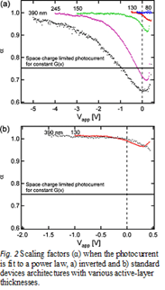 Figure 1
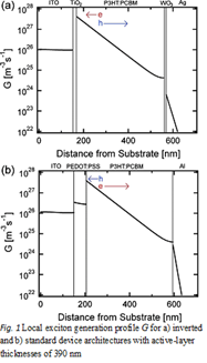
shows G for both inverted and standard solar cells with t = 390
nm and Plight = 10.0 mW/cm2
and 10.9 mW/cm2, respectively. Due to the
high angle 65° and relatively short excitation wavelength ¦Ë = 473 nm, an
exponentially decreasing G profile is set up in the photoactive layer.
Under these conditions, G drops by 3 orders of magnitude from one side
of the active layer to the other for both devices. This type of profile is very
different from those under normal incidence for thinner active layers that vary
by an order of magnitude where the maximum is centered in the middle of the
active layer.
Figure 1
shows G for both inverted and standard solar cells with t = 390
nm and Plight = 10.0 mW/cm2
and 10.9 mW/cm2, respectively. Due to the
high angle 65° and relatively short excitation wavelength ¦Ë = 473 nm, an
exponentially decreasing G profile is set up in the photoactive layer.
Under these conditions, G drops by 3 orders of magnitude from one side
of the active layer to the other for both devices. This type of profile is very
different from those under normal incidence for thinner active layers that vary
by an order of magnitude where the maximum is centered in the middle of the
active layer.
Using this configuration, the average required transport distance for electrons and holes (De,h) is simply set by choosing inverted or standard devices with specific thickness. Determining if De,h set by G are too far for electrons or holes to travel is done by measuring the photocurrent Jphoto = Jlight-Jdark over a range of light intensities Plight and fitting to a power-law relationship Jphoto = b(Plight)a. Because Jphoto describes the current output solely due to photogeneration, the effects of series and shunt resistance that modify electrical performance under illumination are removed and a deviating from ~1 is the signature for bimolecular recombination processes.
Values for a are given in Fig. 2 for both inverted and standard devices with different active-layer thicknesses 80< t <390 nm. It is observed for inverted devices that increasing t causes to deviate from unity for greater reverse bias application i.e., higher internal electric fields. On the other hand, for standard devices with t=130 and 390 nm, remains close to unity over the entire voltage range. Under these illumination conditions with monotonically decreasing G, inverted devices suffer from recombination due to limited free carrier transport while standard devices do not.
The contrasting transport between standard and inverted devices indicates that hole transport is limited for P3HT:PCBM under the prescribed preparation conditions for thicker values of t. This a very important fact that we are now sure. We are taking this into account for the photonic design as transport distances could be quite different inside a patterned active layer both types of charge carriers.
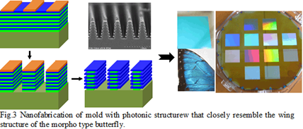
Toward true pine tree-like structures and complex photonic effects.
We fabricated
photonic structures of butterfly wings over large area for the first time using
conventional nanofabrication technology. The photonic nanostructures of
butterfly wings that consists of pine tree-like
periodic multilayer shelf structures standing on multilayer or supporting posts
are fabricated using four simple steps: multilayer deposition,
photolithography, reactive ion etching and wet chemical etching. The parameters
of the pine tree-like structures (e.g., lamellar ridge or pine tree
height, width, number of shelf like lamellae or branches, lamellae width,
thickness and separation) are well controlled and enable us to mimic tree-like
structures of all known butterfly wings. Periodic pine tree-like structures of
various periods (ranging from 500 nm to 3250 nm), various widths (250 nm to
3000 nm), various heights (ranging from 100 nm to 700 nm), lamellae thickness
and separation (50 nm each with various widths up to 3000 nm), and the number
of lamellae (up to seven), are demonstrated to show the control over all the
optical parameters of photonic structure of most of the known butterfly wings.
Optical responses close to that of actual butterfly wings can be
 achieved, thereby demonstrating the possibility of tuning
spectral colors of the resulting nanostructures.
achieved, thereby demonstrating the possibility of tuning
spectral colors of the resulting nanostructures.
This aspect of the project is focusing in the methodology to build these complicated structures (see fig. 3) and later, we bring the expertise to embossing fabrication methods for photonic solar cells enabling a surface texture that truly reflects the inspiration that give rise to the this project. Thanks to the support of the petroleum fund, we have been able to achieve sufficient progress to seed new grant proposals and continue this work.