ACS PRF | ACS
All e-Annual Reports

43557-AC5
High-Resolution Energy Loss Spectroscopy of Sheet Plasmons
Final Narrative Report, 10/01/2007
High-resolution electron energy loss spectroscopy of 'sheet' plasmons
Plasmons are collective modes of excitation of the electronic charge density in solids. At a surface, the truncation of the solid creates a surface plasmon with a frequency lower than that of the bulk, ¦Řp. For a planar surface, the lowering is a factor ¦Řp / °Ě2. Anything that changes the surface charge density affects the surface plasmon, particularly its dispersion behavior, ¦Řsp vs. q, where q is the wavevector of the excitation. In the long wavelength limit q°ú 0, the plasmons cross the light-line ¦Ř=c q and, under the right circumstance, can couple into a light field to generate 'surface polariton' modes. These modes have important application in electro-optic communications and sensing devices. [1]
Plasmons are usually associated with metallic conductors and their frequencies ¦Řp = 4¦Đ ne2/m are high due to the high electron density n, for a silver surface, ¦Řp ~ 1016 s-1 and n ~ 1020 cm-3. Although the associated surface plasmon is confined to a plane, the surface, it is not a strictly two-dimensional excitation. Its electromagnetic field decays slowly, either side of the surface plane, illustrated Fig 1.
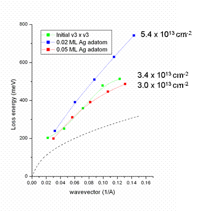
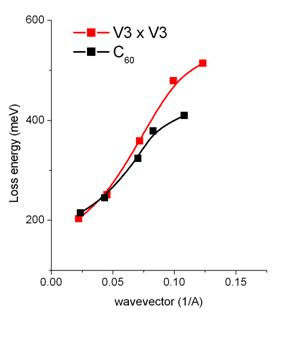
The charge separation generates electric fields between parallel sheets extending into the bulk. The Coulomb restoring force between these sheets is constant with sheet is constant with sheet separation i.e. wavelength ¦Ë. This creates a "frequency gap" at q = 0. Below this frequency ¦Řp/°Ě2, surface plasmons cannot be excited. This is not the case for strictly two-dimensional (2D) plasmons excited on a charged sheet. The wavelength now corresponds to the distance between essentially lines of charge, and the Coulomb force varies logarithmically with separation. Their frequencies vary as °Ěq down to q = 0. [2] These excitations are of considerable scientific interest since their low energies, extending form the far ultraviolet into the far-infrared, allows them to participate in many dynamical processes at surface, They have been observed in nearly two-dimensional (2D) electron-gas systems trapped at the interfaces of semiconductor charge-inversion devices [3] and quantum-well heterostructures. [4] The field-effect transistor has been exploited to vary the electron density down to values as low as n ~ 1010 cm-2 in order to emphasize the electron-electron correlation effect. [5] Enhanced electron-phonon coupling has been reported in these devices, [6] and it is possible they might mediate the formation of cooper pairs in high-transition metal superconductors. 2D plasmons at a 'free' surface were recently reported for metallized silicon surfaces, Si(111) °Ěm °Á °Ěn-M, M= Ag, Au, In, and m, n = integers. The different metal atoms create supperlattice structures with different free electron-densities, ranging from 1011 to 1015 cm-2. We have identified the sheet plasmons on these surfaces and studied their dispersion behavior, as a function of the 2D electron gas density. Fig. 2 The dispersion is a function of the charge density. These 'free surface' systems offer opportunities for studying dynamical processes involving adsorbates. Any charge transfer influences the surface charge density which is seen as change in the dispersion of the sheet plasmons, Fig. 3. An example of the interaction of a monolayer of C60 molecules is shown, Fig. 3 The vibrational frequencies of the molecules can now resonate with the sheet plasmon frequency to produce an enhanced screening of the molecular dipole. Our current research is exploring these and other aspects, of dynamical processes involving 'sheet plasmons'. Preliminary results we presented at an international conference this summer, [7] and being prepared for publication. [8] References: [1] J. Homola, S. S. Yee and G, Gaugitz, "Surface plasmon resonance sensor: a review", Sensors and Actuators B54 3-15 (1999) [2] F. Stern, "Polarizability of a Two-Dimensional Electron Gas", Phys. Rev. Lett. 18, 546 (1967) [3] S. J. Allen, Jr., D. C. Tsui, and R. A. Logan, "Observation of the Two-Dimensional Plasmon in Silicon Inversion Layers", Phys. Rev. Lett. 38, 980 (1977) [4] N. H. March and M. P. Tosi, " Collective effects in condensed conductors phase, including low-dimensional systems", Ad. Phys. 44, 299 (1995) [5] A.V. Chaplik, "Possible crystallization of charge cavras in low-denstiy inversion layers", Sov. Phys. JETP 35, 395 (1972) [6] T. Nagao, T. Hildebrandt, M. Henzler, and S. Hasegawa, "Dispersion and damping of a two-dimensional plasmon in a metallic surface-state band", Phys. Rev. Lett. 86, 5747 (2001) [7] Y. Liu, H. Won and R. F. Willis, "2D Sheet-plasmon behavior and screening at a silicon Schottky barrier interface", Proc. Physical Electronics Conf, Urbana-Champaign, 2007, Abstract #4 [8] Y. Liu and R. F. Willis, "High momentum-resolution electron energy loss measurements of sheet-charge plasmons on metallized silicon surfaces", in preparation. 

