
ACS PRF | ACS
All e-Annual Reports

43989-G10
Charge Transfer in Organic Semiconductors: From Microscopic to Macroscopic Electronic Properties on all Time Scales
The goals of our project are to understand charge carrier dynamics in high-performance organic semiconductors and to lay foundations for charge-transfer-based single-molecule optoelectronic devices. This is of importance not only for improvements in electronic materials design and device performance, but also could lead to breakthroughs in nanoscale electronics and charge-transfer-based biological applications. Of particular interest is the relationship between macroscopic conductivity and microscopic charge-transfer rates. To achieve these goals, we use carefully designed organic semiconductors and a variety of time-resolved techniques including transient photocurrent and fluorescence spectroscopy in combination with single-molecule-level fluorescence imaging.
The materials suitable for our studies must exhibit: (i) high photoconductivity, (ii) either very strong or complete lack of fluorescence, and (iii) fluorescent properties depending on the charge state of the molecule. The materials that satisfy the above requirements are high–performance functionalized pentacene (Pc-TIPS), functionalized anthradithiophene (ADT-TIPS-F), and dicyanomethylenedihydrofuran (DCDHF) derivatives (inset of Fig.1). Polycrystalline Pc-TIPS and ADT-TIPS-F and amorphous DCDHF films are drop-cast from toluene. For macroscopic photoconductivity studies, films are deposited on a glass substrate with photolithographically patterned aluminum interdigitated electrodes (inset of Fig.1(a)).
When voltage is applied, and the samples are excited by a 100-fs 400-nm laser pulse, charge carriers photogenerated in the films move under the electric field, creating a current registered by a 50-GHz digital sampling oscilloscope. All materials under study exhibit fast carrier photogeneration (<30 ps, limited by time resolution of our setup), charge-trap-density-dependent photocurrent decay (Fig.1(a)-(b)) and bandlike charge (hole) transport characterized by charge carrier mobility increasing with decreasing temperature, similar to that in GaAs (Fig.1(c)). We also observe electric field-assisted charge detrapping that modifies decay dynamics on ps time scales (Fig.1(b)) and light-induced trap filling effect. When a low concentration of one derivative (e.g. ADT-TIPS-F) is introduced into a matrix made of a different derivative (e.g. Pc-TIPS), charge trapping properties of the matrix can be changed, depending on the difference between ionization potentials of the matrix and dopant molecules. Since slight chemical modifications allow for tuning of the ionization potential of a molecule, we can introduce traps of variable depths, energetic and structural, polar (e.g. DCDHF) and non-polar (e.g. ADT-TIPS-F), into a matrix (e.g. Pc-TIPS) in a controlled way. This changes decay dynamics in Fig.1(a) and allows us to model charge trapping properties.
Outcomes:
At this stage of the project, we built all necessary experimental setups and completed studies of charge carrier dynamics in the bulk (ensemble) systems (macroscopic conductivity in thin-film devices) and of fluorescent properties of derivatives promising for microscopic-level studies. In particular, we observed:
- Fast charge carrier generation (<30 ps, limited by time resolution of our setup)
- Bandlike transport, similar to that in GaAs, from picoseconds (ps) to milliseconds (ms) after photoexcitation in polycrystalline Pc-TIPS and ADT-TIPS-F films
- Film morphology- and structure-dependent decay of the transient photoconductivity: e.g. most photogenerated charges are trapped within ~200 ps in DCDHF amorphous glass, while those in Pc-TIPS and ADT-TIPS-F propagate in extended states at least up to ~50 ms after photoexcitation;
- Electric field-assisted emptying of shallow traps in films with a lower trap density (e.g. ADT-TIPS-F)
- Light-induced charge trap filling effect in all films
- Fluorescence lifetimes of 2-10 ns, depending on the derivative
- Fluorescence lifetime reduction in films (solid-state) compared to solutions
- Quenching of the fluorescence upon oxidation, crucial for our experiments at microscopic scales
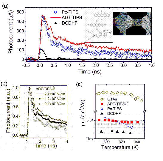
Figure 1. (a) Transient photocurrent in Pc-TIPS, ADT-TIPS-F and DCDHF thin films. Inset: molecular structures of the Pc-TIPS, ADT-TIPS-F and DCDHF molecules (top to bottom, respectively). Pc-TIPS film deposited onto a glass substrate with photolithographically patterned interdigitated electrodes is also shown. (b) Normalized transient photocurrent observed in ADT-TIPS-F films at various electric fields. (c) A product of charge carrier mobility (μ) and photogenerated efficiency (η) calculated from the peak value of the photocurrent measured in GaAs and Pc-TIPS, ADT-TIPS-F and DCDHF films as a function of temperature.
Our next stage is studies of charge-transfer properties in these materials at nanoscales and their relation to charge carrier dynamics observed in bulk materials. 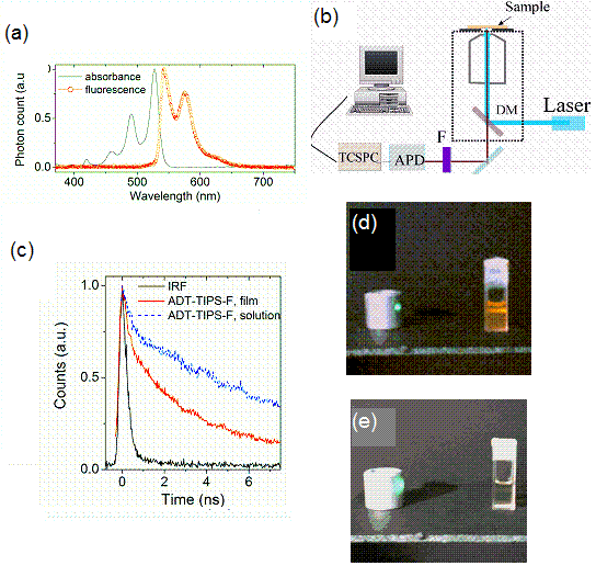
Figure 2. (a) Normalized absorbance and fluorescence of the ADT-TIPS-F derivative in toluene. (b) Schematics of the experimental setup used in time-resolved fluorescence measurements. (c) Time-resolved fluorescence decay in ADT-TIPS-F thin film and solution. The instrument response function (IRF) is also shown. (d) and (e) : Change of fluorescence upon oxidation of the DCDHF molecules: (d) highly fluorescent neutral DCDHF and (e) non-fluorescent DCDHF+ cations.