Reports: AC10
45359-AC10 Sonoelectrochemical Approach Towards Novel Nanostructured Thermoelectric Materials
Cu2-xS (x = 1, 0.2, 0.03) nanocrystals are interesting materials due to their disordered cation distribution, that makes these interesting materials for thermoelectric applications. We have synthesized Cu2-xS nanocrystals with three different chemical methods: sonoelectrochemical, hydrothermal, and solventless thermolysis methods in order to compare their common optical and structural properties and to subsequently better understand their potential for thermoelectics. The crystallinity and morphology of the products were characterized by XRD and transmission electron microscopy (TEM), which shows that most products are of pure stoichiometries but some of them are also mixtures. The obtained XRDs were studied in comparison to the XRD patterns of previously reported Cu2-xS. We found consistently that under ambient conditions the copper deficient Cu1.97S (djurleite) is more stable than Cu2S (chalcocite). Corroborated by recent computational studies by Lambrecht et al. and experimental work by Alivisatos et al. This may be the reason behind the traditionally known instability of the bulk Cu2S/CdS interface. Both Cu2S and the copper-deficient Cu1.97S have very similar but distinguishable electronic and crystal structure. The optical properties of these Cu2-xS NCs were characterized by UV-vis spectroscopy and NIR. All presented Cu2-xS NCs show a blue shift in the band gap absorption compared to bulk Cu2-xS. Moreover the spectra of these Cu2-xS NCs indicate direct band gap character based on their oscillator strengths, different from previously reported experimental results. The NIR spectra of these Cu2-xS NCs show a carrier concentration dependent plasmonic absorption, indicating a transition from a semiconductor material to a quasi-metallic material. Such high carrier densities are typical for thermoelectric materials. This work was published in JACS, 2009.
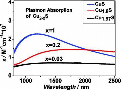
Figure 1.The plasmonic Absorption of Cu2-xS nanocrystals depends on the composition and carrier concentrations.
In a second study, we synthesized Bi0.5Sb1.5Te3 nanocrystals. The thermoelectric (TE) properties of the synthesized Bi0.5Sb1.5Te3 nanocrystals (NCs) were modified by annealing under the protection of Ar. The improvement of the thermoelectric performance of chemically synthesized Bi0.5Sb1.5Te3 and Bi2Te3 NCs was realized by increasing the thermoelectric powerfactor (S2σ), especially the electrical conductivity σ, and maintaining their lower lattice thermal conductivity (κL) due to their nanoscaled grain boundary after appropriate annealing. Hall carrier concentration investigation suggested that the improvement on electrical conductivity is dominated by modification on extrinsic properties (charge carrier mobility) rather than intrinsic properties (carrier concentration). A plausible mechanism for the modification of the charge transport character from semiconducting to metallic and for a large increase of the mobility by annealing was proposed to explain the significant modification. The lattice thermal conductivities of Bi2Te3 and Bi0.5Sb1.5Te3 NCs after annealing still show relatively lower value compared to bulk one, which is due to their nanoscaled grain boundary as confirmed by SEM. These result demonstrated the potential power of chemically synthesized TE nanomaterial after appropriate post-treatment. The synthesis part of this work has been published in ACS Applied Materials & Interfaces (2009).
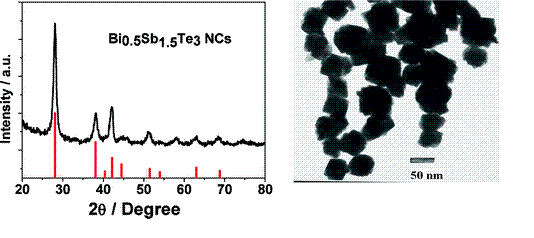
Figure 2.XRD and TEM of Bi0.5Sb1.5Te3 nanocrystals.
Transport properties of Bi2Te3 and Bi0.5Sb1.5Te3 NC pellets
A) Bi2Te3 NCs
Vacuum dried Bi2Te3 NC pellets (no annealing) have a room temperature electrical conductivity of 30.1 S/cm. Although lower than the reported value for optimized bulk Bi2Te3 (around 1000 S/cm), this value is comparable to previously reported annealed chemically synthesized Bi2Te3 NCs. The electrical conductivity increases with temperature, indicating semiconducting or activated behavior. The room temperature Seebeck coefficient (S) value is -69.2 μV/K, which indicates that these Bi2Te3 NCs are n-type semiconductors. After 300 °C annealing, the room temperature values of σ and S both increased to 58.9 S/cm and -120μV/K, respectively. As a result, the room temperature power factor (σ*S2) increased about six times compared to the vacuum dried sample. We note that the nominal expectation is that S should decrease if s increases, assuming the cause is due to an increase in carrier concentration. However, a simultaneous increase in s and S was also seen in the other chemically synthesized Bi2Te3 NCs. We propose that as the thiol capping layers are removed from the individual NPs during annealing, the carrier mobility in the pressed pellet has drastically increased, leading to much improved properties. After 350 °C annealing, the room temperature σ increased to 112.4 S/cm but the room temperature S value decreased. The power factor of 350 °C annealed Bi2Te3 NCs was almost the same as that of 300 °C annealed Bi2Te3 NCs. The room temperature electrical conductivity of 380 °C annealed Bi2Te3 NCs jumped to 570.3 S/cm, which is a high value for chemical synthesized Bi2Te3 NCs. While S decreased further with increasing temperature, the 380 °C annealed sample still showed the highest power factor, sixteen times larger than vacuum dried Bi2Te3 NCs, due to the large s.
B) Bi0.5Sb1.5Te3 NCs
The unannealed Bi0.5Sb1.5Te3 NCs also have a relatively lower room temperature electrical conductivity of 26.1 S/cm, as shown in Figure 3, compared to the state of art reported value of optimized bulk Bi0.5Sb1.5Te3, around 1000 S/cm. The room temperature Seebeck coefficient of the vacuum dried Bi0.5Sb1.5Te3 NCs is 127.2 μV/K, which indicates that these Bi0.5Sb1.5Te3 NCs are p-type semiconductors. Both s and S increased in annealed samples at each temperature step up towards 380 °C. The Seebeck coefficient reached its maximum value of 256.6 μV/K for this annealing temperature. The 400 °C annealed Bi0.5Sb1.5Te3 NC sample has a much higher room temperature s of 251.6 S/cm, while the room temperature S value decreases slightly. Like the Bi2Te3 NC samples, the conductivity has an activated character over the entire temperature range except at the highest annealing temperature, indicating a possible change in conductivity mechanism. The power factor increased monotonically with annealing temperature, reaching a maximum value of 13.8 mSV2cm-2K-2, which is over 30 times greater than the unannealed Bi0.5Sb1.5Te3 NC sample. These findings are currently being written up and will be published within 2009.
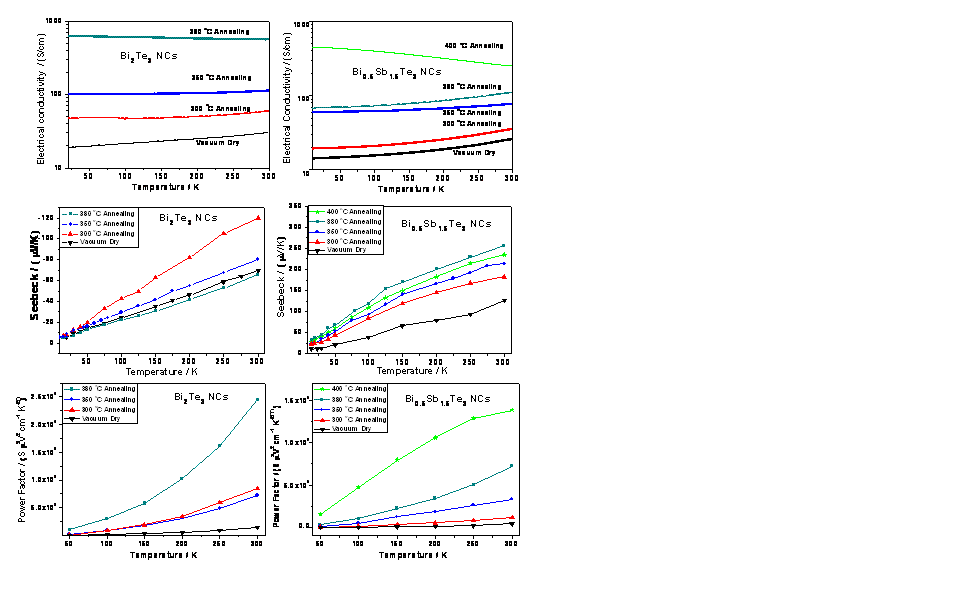
Figure 3. Electrical conductivity (σ), Seebeck coefficient (S) and power factor (σ*S2) of Bi2Te3 NCs and Bi0.5Sb1.5Te3 NCs.