Reports: G10
46777-G10 Fundamental Investigations of the Microstructure of Semicrystalline Polymers for Alternative Energy Generation
There has been great interest recently in structure-property relationships of conjugated polymers. Indeed, this class of materials has found applications in the fabrication of low-cost electronic devices such as thin-film transistors, light-emitting diodes or photovoltaic cells. The two latter applications are of particular relevance in tackling the energy challenge. Light-emitting diodes can potentially replace incandescent or fluorescent light bulbs leading to energy conservation. Photovoltaic cells on the other hand can be used to produce cheap energy from sunlight. The goal of the proposed research was to study the microstructure of organic/inorganic interfaces by transmission electron microscopy (TEM). While we were able to produce TEM foils of organic/inorganic interfaces (pentacene/SiO2), the preparation method (focused-ion beam cutting) inevitably led to the amorphization of the organic semiconductor (Fig. 1).
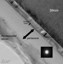
Figure 1: cross-sectional TEM of an Al/Al2O3/pentacene stack. The inset is an electron diffraction pattern taken in the pentacene layer showing lack of crystalline order.
As a result, we turned our attention to sample preparation methods that did not involve energetic ion beams. Furthermore, we decided to undertake TEM analysis of semiconducting polymers as these are more promising, compared to small molecule materials, for the fabrication of low-cost photovoltaics by solution processing. We chose the most crystalline semiconducting polymer available PBTTT. PBTTT also exhibits the highest mobility of all semiconducting polymers and is therefore of interest for bulk heterojunction photovoltaics.
Spin coated thin films of PBTTT were delaminated off the silicon substrate coated with octadecyl-trichlorosilane (OTS), floated off and deposited on TEM grids. The TEM analysis was carried out at room temperature using a Tecnai F20 TEM (FEI Company) using low-dose operating conditions at 200kV acceleration voltage. The specimens were not particularly beam sensitive, however, after longer or intense exposure, damage to the specimen could be observed. Hence, focusing and beam adjustments were made on "sacrificial" regions of the film in order to induce minimal beam and image shift. This low-dose approach prevented the more interesting areas from unwanted and unnecessary exposure to the electron beam. Yet, to still record images with acceptable image contrast, the electron dose per recorded image was adjusted to vary between 40 and 50 e- -2. To investigate the crystallinity of annealed PBTTT, films spun-cast on OTS-treated SiO2 were characterized by TEM. The TEM images reveal the existence of nanoscale features (ca. 10 nm in size) in the PBTTT film (Figure 2a). This observation is in stark contrast with AFM characterization of PBTTT films cast on OTS-treated SiO2, which exhibit large flat terraces and molecular-height steps after annealing into the polymer's mesophase. In AFM terraces are clearly visible, with lateral sizes of the order of 250-300 nm, much larger than the characteristic feature size observed by TEM (Figure 2b).
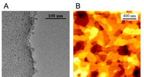
Figure 2: TEM micrograph of a PBTTT film (a) and AFM scan of a film of the same material prior to TEM preparation.
TEM characterization strongly suggests that the PBTTT terraces are composed of smaller microstructural subunits of a characteristic size (~10 nm) similar to that of microstructural features observed in other semicrystalline polymers.These subunits are crystalline because they are not observed in unannealed films, that have low crystallinity according to X-ray diffraction measurements. Furthermore, the orientation contrast of neighboring grains in the TEM changes independently with sample tilt, as expected in polycrystalline films. Finally, fracture lines at the film edges are predominantly intergranular. Single crystal diffraction could not be obtained because of the weak scattering of the polymer, the non-perfect flatness of the film combined with the sensitivity of the film to the electron beam. In order to obtain sufficient contrast the images are approximately 500 nm out-of-focus, which prevents us from making quantitative estimates of the amount of defective material. It should be noted however that the nanoscale features are not due to artifacts introduced by sample preparation because they are not observed in the identically-prepared unannealed films imaged in the same conditions.
In summary, the TEM study reported here allowed to reveal the true microstructural lengthscales of PBTTT and provided a better understanding of the charge transport limitations in this material.