Reports: AC5
47099-AC5 Hydrogenation Reactions on Palladium Involving Subsurface Hydride
We have been investigating the interactions of deuterium and the sulfur-containing heterocycle, thiophene, on Pd{111} and Pd{110} at 4 K by ultrahigh vacuum scanning tunneling microscopy (STM). Previously, we observed these species on the Pd{111} surface and reported initial findings of single-molecule vibrational spectroscopy (inelastic electron tunneling spectroscopy, IETS). Here, we report on the diffusion of deuterium on Pd{111} at 4 K as a consequence of tunneling electrons, and on the influence of the {110} surface on adsorption and potential substrate-mediated interactions (SMI). We are continuing to develop the methods for carrying out and monitoring dynamically the reactions of single molecules with surface-bound hydrogen, subsurface hydride, surface-bound deuterium and subsurface deuteride. We propose that the SMI between thiophene molecules on the D-covered Pd{110} surface provide a novel route toward guiding molecular reactants into proximity for tip-induced hydrogenation reactions.
Previously, we showed that H adatoms are mobilized on Pd{111} at 4 K at a tunneling electron onset voltage of ±0.1 V (i.e., at 0.1 eV electron energy) [1]. We explained this activated motion in terms of a tunneling-electron-induced process. Here, we have performed analogous studies on D adatoms. Figure 1A-C highlights three sequential images of D on Pd{111} acquired at a sample bias of 0.1 V, with Figure 1D showing the correlation of motion from the image sequence. Motion was apparent, and was examined in detail by compiling more than 200 sequential image frames. We find that the onset for diffusion is approximately ±0.07 V for the D adatoms, and that they exhibit significantly more diffusion at ±0.1 V, particularly in regions where individual D adatoms have fewer nearest neighbors. Proximity effects are no doubt important and can be quantified using techniques that we have developed.
We have performed differential conductance imaging of thiophene on the bare Pd{110} surface at 4 K to study electronic structure and substrate influences. Figures 2A and 2B show the topographic and differential conductance images, respectively, of a cluster of thiophene adsorbates. Because differential conductance measures the local density of states, we are able to probe empty or filled states, depending on the polarity of the applied bias. As observed in Figure 2B, we can observe the electronic structure of the molecules directly. In the future, we will employ this technique to distinguish reaction products from intermediates and reactants when we perform tip-induced hydrogenation reactions.
We have acquired IETS of single thiophene molecules on Pd{110}. Figure 3 shows the IETS signature averaged from 200 individual spectra. We assign the highlighted vibrational bands (between ±0.13 eV and ±0.18 eV) to be a convolution of the four vibrations previously observed for thiophene on γ-Al2O3 by Quigley et al. using infrared spectroscopy (Table, Figure 3) [2]. Because IETS requires that a molecular vibration have a vector component normal to the surface, we postulate that the thiophene molecules adsorb with upright or tilted orientations. We are currently optimizing IETS parameters to resolve individual vibrational peaks within these bands. Differentiation of the individual peaks will yield additional insight into the selection rules for IETS, and will provide us a powerful tool for monitoring the reactants and products of tip-induced reactions.
We have observed the possible effects of SMI on the relative adsorption sites for sub-monolayer coverages (0.0018 molecules/Å2)
of thiophene on Pd{110}. As the STM image in the inset of Figure 4 indicates,
the distribution of thiophene molecules does not appear random, but instead
shows preferential separations between the molecules. From 50 images like that
in Figure 4, we have measured over 600,000 relative distances, which we have
compiled into the normalized histogram shown in Figure 4. This histogram
demonstrates oscillatory behavior of the probability of finding a neighboring
molecule P(r) at a distance (r). We note that for a given
molecule, the highest probability for finding a neighbor is at 8.8 Å instead of
at 2.75 Å, which is the nearest neighbor distance of Pd surface atoms in the
<1![]() 0> direction. At this time,
we are using differential conductance imaging to measure the wave vector of the
bare Pd{110} surface state in order to determine if the separations observed in
the histogram of Figure 4 can be explained by the electronic structure of this
surface.
0> direction. At this time,
we are using differential conductance imaging to measure the wave vector of the
bare Pd{110} surface state in order to determine if the separations observed in
the histogram of Figure 4 can be explained by the electronic structure of this
surface.
[1] L. C. Fernandez-Torres, E. C. H. Sykes, S. U. Nanayakkara, and P. S. Weiss, Journal of Physical Chemistry B 110, 7380 (2006).
[2] W. W. C. Quigley, H. D. Yamamoto, P. A. Aegerter, G. J. Simpson, and M. E. Bussell, Langmuir 12, 1500 (1996).
Figures
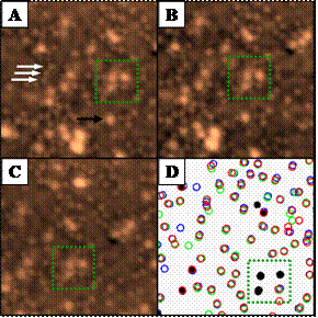
Figure 1. (A-C) Sequential STM topographic images (90 Å × 90 Å, Vs = 0.1 V, It = 50 pA)
acquired over a region of D (white arrows) on Pd{111} at 4 K. The protrusions
(black arrow) are impurities in the Pd substrate. (D) D adatoms are
highlighted and correlated using an automated technique
(A - blue, B - green, C - red). The green dashed
squares highlight the reference area (black filled circles in D).
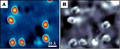
Figure 2. A) STM topographic image (70 Å × 60 Å, Vs = 0.1 V, It = 900 pA) of thiophene molecules on Pd{110}. B) STM differential conductance image of the same molecules. These images were acquired simultaneously.
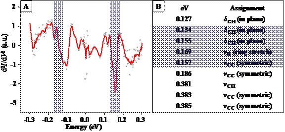
Figure 3. A) Inelastic electron tunneling spectrum of a single thiophene molecule on Pd{110}, averaged from 200 individual spectra. B) Table listing the vibrational mode assignments of thiophene on γ-Al2O3, as measured by Quigley et al. using infrared spectroscopy [2].
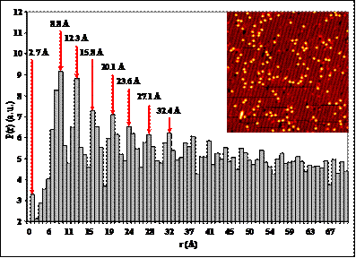
Figure 4. Normalized
histogram of separations between thiophene molecules on Pd{110}
(0.0018 molecules/Å2) determined from a series of 50 non-overlapping STM images recorded at 4 K. The inset shows a representative STM image (280 Å × 280 Å, Vs = 0.01 V, It = 900 pA) used for
the separation measurements.