Reports: G10
47721-G10 Advanced Transparent Conducting Materials for Thin Film Solar Cells
As photovoltaic (PV) technology continues to mature, research beyond the active PV material is becoming more critical. One such area involves transparent conducting (TC) materials. TC's are an integral part of a solar cell. More and more, as the basic materials science issues are solved for the active PV materials, higher demands are placed upon the associated materials. TC's are no exception. The most common material, tin-doped indium oxide, is no longer the âbest' material for a given solar cell. The demands on TC's have increased beyond conductivity and transparency alone. And, with the exceedingly high cost and demand of indium, the PV community is in desperate need of a functional replacement. This program was designed to explore a suite of material systems suitable for replacing current TC materials. New and existing compositions were to be investigated and implemented on the basis of transparency, conductivity, resistance to diffusion, thermal and chemical stability, and microstructure. The main initial objectives of this program were the following:
1) Explore alternative and existing transparent conducting materials systems and deposition methods
2) Utilize âengineered' microstructures to artificially enhance the properties
3) Implement these new TC materials systems in real PV devices
In order to move towards accomplishing these objectives, the priorities of the first year and a half of this program centered on developing chemical and physical vapor deposition capabilities.
To this end, the majority of the funds allocated thus far have gone towards the construction of two main deposition facilities. Both are recently completed and are currently being used to advance the initial goals of the program. Figure 1 shows a multi-target RF-magnetron sputter deposition system. This system has capabilities for heated (up to 850 °C in oxygen) deposition. It is designed with a 2 in. and a 1 in. diameter target, which provides the ability for co-sputtering. In addition, we have capabilities to fabricate 1 in. targets, thus new materials exploration can occur in a very rapid fashion.
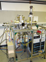
Figure 1: RF-magnetron sputter system
Although RF-sputtering is a scalable technology (and widely used in industry), it does not always provide the simplest initial pathway to new materials deposition. Thus, to introduce an even more flexible deposition technique, funds from this program were used in concert with an equipment donation from Los Alamos National Laboratory (via the Laboratory Educational Equipment Grant) to construct an ozone assisted pulsed laser deposition (PLD) system. This system is shown in figure 2. PLD offers a very simple route to thin films of complex oxides, as it is essentially a âflash evaporation' process. The general disadvantage to the technique is a limitation in scalability. However, as new materials are identified they can be transferred to the RF-sputtering system described above. The advantage of in-house target fabrication is also relied upon here.
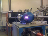
Figure 2: Pulsed Laser Deposition system.
Although these systems have been constructed in large part with funds from this program, it is important to note that they will exist long after this work is completed. Already they have impacted my research group via increased collaboration across our campus and with other institutions. This is an area of critical importance to the future of research in my group and the development of follow-on funding.
Initial materials development is focused on ZnO and doped-ZnO thin films. Figure 3 shows an x-ray diffraction pattern and scanning electron micrograph of a 300 nm thick film deposited via RF-magnetron sputtering. c-axis orientation is achieved with a dense microstructure. Optimization of film growth is currently underway, with subsequent experiments planned to observe impurity diffusion as a function of grain size in the ZnO films.
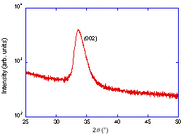
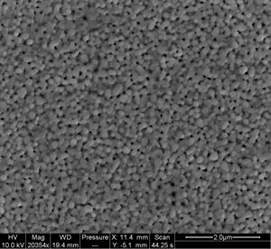
Figure 3: X-ray diffraction pattern and scanning electron micrograph of an rf-sputtered ZnO thin film.
From an educational standpoint this program has also had an unexpected significant impact. In the spring of 2007 we introduced a new course -- "Experimental Techniques in Materials Science." This is a laboratory class, with modules designed to introduce students to various methods of fabrication and characterization of materials. Each offering is designed around a specific material. For this first year the topic was tin-doped indium oxide (the transparent conductor ITO). The methods developed in my laboratory to deposit ITO for our research were extended to this class, and students were able to understand the importance of transparent conducting materials (no funds were directly used for the class).
Finally, I have attempted to include undergraduate researchers on this project whenever possible. I have paid for one student using these funds, with others coming from work-study programs. Results from one student's work led to a submission to Oregon State University's Undergraduate Research, Innovation, Scholarship, and Creativity (URISC) program, which provides additional funding for the student. Although this attempt was unsuccessful in the end, he is still working on this program and will likely try again this coming year.
It is clear there is still much to be done towards accomplishing the initial goals of this program. With the infrastructure now in place I expect significant progress to occur over the coming year. Through separate research programs I have recently added capabilities for spectroscopic ellipsometry and atomic force microscopy. Both of these tools will be very useful as we pursue development and characterization of new and existing transparent conducting materials.