Reports: B10
46713-B10 Exploring Defect Level Position and Occupation in Metamorphic Heterostructures for Multi-junction Photovoltaic Converters
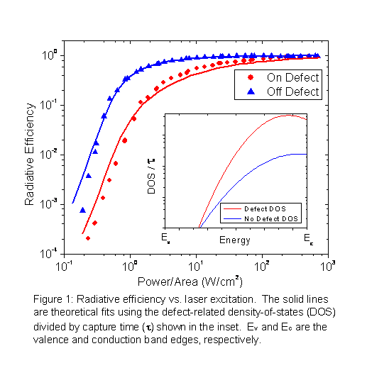
Our group had another productive summer investigating the properties of defects in semiconductors. Last summer, we began a new experiment, using a high performance camera to image semiconductor photoluminescence. We observe darkened regions near isolated defects (presumably dislocations) in GaAs due to augmented non-radiative recombination. These depleted regions expand as we reduce the excitation intensity, increasing the average diffusion length and allowing more distant carriers to diffuse to the defect. This summer, we continued the photoluminescence imaging project on two fronts. A new student in our group, Caroline Vaughan, made excitation-dependent radiative efficiency measurements near and far from an isolated defect. She is using these measurements to obtain a more accurate picture of defect-related recombination in GaAs. In particular, these results provide information on how the density, energy, and capture time of defect-related states are different near crystal dislocations (see Figure 1 for an example of this analysis).
In the meantime, returning student Mac Read is trying to incorporate these results into a computational model of diffusion and recombination in the vicinity of the defect. Both of these students are continuing their research during the 2009-10 academic year with the goal of writing honors theses on their accomplishments and graduating in the spring with honors in physics. In 2010, we hope to bring all of this work together to formulate a complete, self-consistent picture of how dislocations impact the motion and recombination of photo-excited charge carriers in solar cell materials. Caroline and Mac both plan to attend engineering graduate school next year.
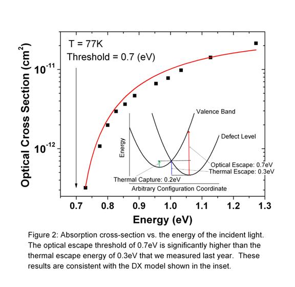
My other returning student, Dan Hampton, continued his transient capacitance measurements by adding a powerful new capability to the experiment a widely tunable source of monochromatic light. Our previous work on GaAsP and GaInP diodes indicated that a class of defects often referred to as DX centers were active in these devices. Because the configuration of the lattice around the defect changes when the defect state is occupied, the electrical, thermal, and optical properties of the defect are more complicated. Dan investigated the optical response this summer, and his results are consistent with the DX model (see Figure 2 for Dan's measurement of the optical activation threshold in the GaInP).
Since this type of defect is usually centered on a donor atom, we were surprised to find evidence of it in the p-type region of our test structures. However, our collaborators at the National Renewable Energy Lab have recently confirmed (via secondary ion mass spectroscopy) that the n-type dopant (sulfur) in our diode is diffusing across the junction into this region of the device. This diffusion process appears to be facilitated by the crystal dislocations in these lattice-mismatched structures. We now believe that we have a good understanding of what is happening in these alloys, which should facilitate better solar cell designs incorporating these alloys in the future.