Reports: AC5
47304-AC5 Structures and Defects at Interfaces in Organic Molecular Heterostructures
Thin films of molecular organic semiconductors present the tantalizing opportunity to develop thin film materials with optimized properties for applications in optoelectronics and photovoltaics. Small-molecule semiconductors transport charge over relatively long distances with high carrier mobilities. These high mobilities in turn result in relatively long diffusion lengths for the excitons created by the absorption of light. It has long been recognized, however, that the mobility of carriers in thin films is far lower than in single crystals of the same materials. For molecules such as pentacene the difference can be an order of magnitude or more. A commensurate increase in the exciton diffusion length would be extremely valuable in light-harvesting applications. We have begun a comprehensive study of the structural defects that limit in the mobility of carriers in these thin film structures. The first element of our study involves probing the defects that arise in the formation of thin films of the small-molecule semiconductor pentacene. Here we have probed the structural relaxation of the pentacene lattice near vacancies and identified a variety of previously unreported defects. Defect structures at interfaces pose a more complicated structural problem that we have begun to approach by studying the interface between pentacene and the dipolar molecule nitrobenzene.
Vacancies
Depositing pentacene molecules on Si surfaces terminated by
a monolayer of styrene molecules pentacene crystal that are structurally
similar to those grown on insulating substrates, but which are sufficiently
smooth and conductive for
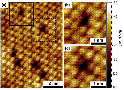
Figure 1 (a)
Extended structural defects
The growth of pentacene thin films also results in a variety
of extended structural defects including dislocations, grain boundaries, and stacking
faults. We have used
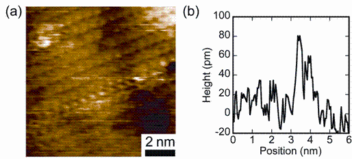
Figure 2 (a)
As part of the preparation of the silicon surfaces for these
studies of pentacene crystals, we have observed the formation of a new class of
nanostructures on silicon-on-insulator surfaces. These structures are stepped rectangular
truncated pyramids, with lateral dimensions of tens of nanometers,
that form on the outer Si layer of ultra-thin (001)-oriented
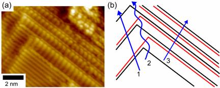
Figure 3 (a) A corner of a nanostructure formed by annealing
a
Conclusion and Future Directions
We are now beginning to study the formation of interfaces using this approach, beginning with the interface between pentacene and the polar surface passivation layer nitrobenzene. The identification of defects associated with these interfaces and of the structure of the interfaces themselves promises to be an important step in the development of organic semiconductor devices incorporated layered small molecule structures.